|
|
|
|
1
|
|
2
|
|
3
|
Click Add.
|
|
4
|
Click Add.
|
|
5
|
Click
|
|
6
|
|
7
|
Click
|
|
1
|
In the Model Builder window, under Component 1 (comp1) > Electromagnetic Waves, Frequency Domain (emw) click Wave Equation, Electric 1.
|
|
2
|
|
3
|
|
1
|
In the Model Builder window, under Component 1 (comp1) > Electromagnetic Waves, Frequency Domain 2 (emw2) click Wave Equation, Electric 1.
|
|
2
|
|
3
|
|
1
|
|
2
|
|
1
|
|
2
|
|
3
|
|
4
|
|
5
|
|
6
|
|
7
|
|
8
|
Click to expand the Layers section. In the table, enter the following settings:
|
|
9
|
|
10
|
Select the Right checkbox.
|
|
11
|
Select the Front checkbox.
|
|
12
|
Select the Back checkbox.
|
|
13
|
Clear the Bottom checkbox.
|
|
14
|
Select the Top checkbox.
|
|
15
|
Locate the Selections of Resulting Entities section. Select the Resulting objects selection checkbox.
|
|
16
|
|
1
|
|
2
|
|
3
|
|
4
|
|
5
|
|
6
|
|
7
|
|
8
|
Locate the Layers section. In the table, enter the following settings:
|
|
9
|
|
10
|
Select the Right checkbox.
|
|
11
|
Select the Front checkbox.
|
|
12
|
Select the Back checkbox.
|
|
13
|
Locate the Selections of Resulting Entities section. Select the Resulting objects selection checkbox.
|
|
14
|
Click
|
|
15
|
|
1
|
|
2
|
|
3
|
|
4
|
Locate the Selections of Resulting Entities section. Select the Resulting objects selection checkbox.
|
|
5
|
|
6
|
Click the
 |
|
1
|
|
2
|
|
1
|
|
2
|
|
3
|
|
4
|
|
5
|
|
1
|
|
2
|
|
3
|
|
4
|
Locate the Scaling section. From the Physics list, choose Electromagnetic Waves, Frequency Domain 2 (emw2).
|
|
1
|
In the Model Builder window, under Component 1 (comp1) right-click Definitions and choose Variables.
|
|
2
|
|
3
|
|
4
|
|
5
|
Locate the Variables section. In the table, enter the following settings:
|
|
1
|
In the Model Builder window, under Component 1 (comp1) right-click Materials and choose Blank Material.
|
|
2
|
|
3
|
Locate the Material Contents section. In the table, enter the following settings:
|
|
1
|
|
2
|
|
3
|
|
4
|
Locate the Material Contents section. In the table, enter the following settings:
|
|
1
|
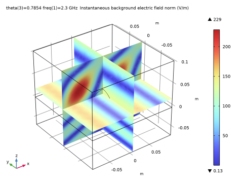
In the Model Builder window, under Component 1 (comp1) click Electromagnetic Waves, Frequency Domain (emw).
|
|
2
|
In the Settings window for Electromagnetic Waves, Frequency Domain, locate the Domain Selection section.
|
|
3
|
|
1
|
|
3
|
|
4
|
|
5
|
|
6
|
|
1
|
|
2
|
|
3
|
Click
|
|
5
|
|
1
|
|
3
|
|
4
|
|
5
|
|
1
|
|
2
|
|
3
|
Click
|
|
1
|
In the Model Builder window, under Component 1 (comp1) click Electromagnetic Waves, Frequency Domain 2 (emw2).
|
|
2
|
|
3
|
From the list, choose Scattered field.
|
|
4
|
|
1
|
|
2
|
|
3
|
|
1
|
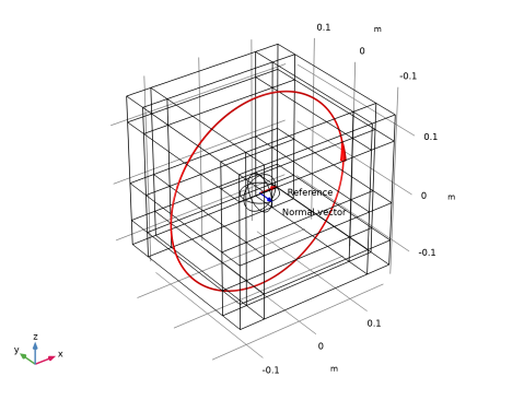
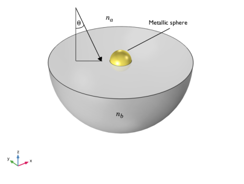
In the Model Builder window, expand the Far-Field Domain, Inhomogeneous 1 node, then click Substrate 1.
|
|
1
|
|
2
|
|
3
|
|
4
|
Locate the Physics and Variables Selection section. In the Solve for column of the table, under Component 1 (comp1), clear the checkbox for Electromagnetic Waves, Frequency Domain 2 (emw2).
|
|
1
|
|
2
|
|
3
|
In the Solve for column of the table, under Component 1 (comp1), clear the checkbox for Electromagnetic Waves, Frequency Domain (emw).
|
|
4
|
In the Solve for column of the table, under Component 1 (comp1), select the checkbox for Electromagnetic Waves, Frequency Domain 2 (emw2).
|
|
1
|
|
2
|
|
3
|
Click
|
|
5
|
|
1
|
|
2
|
|
3
|
|
4
|
|
1
|
|
2
|
|
3
|
|
4
|
|
1
|
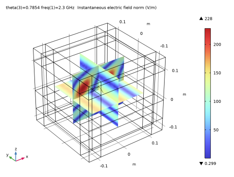
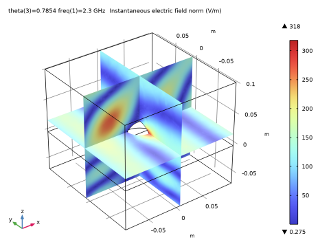
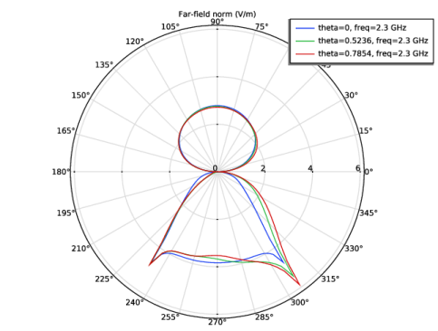
In the Model Builder window, expand the Results > 2D Far Field (ffi1) node, then click Radiation Pattern 1.
|
|
2
|
|
3
|
|
4
|
|
5
|
|
6
|