PDF

Dielectric Resonator Antenna
Introduction
A slot-coupled dielectric resonator antenna (DRA) utilizes a dielectric resonator to enhance radiation and bandwidth. By incorporating a slot in the ground plane to couple with the resonator, this design achieves effective impedance matching and signal efficiency, making it ideal for compact, high-frequency applications such as wireless communications and radar.
Figure 1: Slot-coupled dielectric resonator antenna. The surrounding PML is not visualized.
Model Definition
A slot antenna is created by removing a rectangular section from a ground plane. This slot antenna is excited by a 50 Ω microstrip line, which is connected to a lumped port simulating the power source. The microstrip line is shorted to one edge of the slot, functioning similarly to an open-end quarter-wave stub. To simplify the computation, both the ground plane and the microstrip line are treated as geometrically thin and lossless, and are modeled as perfect electric conductor (PEC) surfaces.
Above the slot antenna, a block of quartz dielectric is positioned. This block serves both as a resonant structure and as a radiating element. The entire antenna setup is enclosed within a sphere representing a vacuum. The sphere is bounded by a perfectly matched layer (PML) domain, which acts as an open boundary for the free space.
Results and Discussion
The antenna structure is analyzed for operation at frequencies approximately around 10 GHz. The resulting far-field radiation patterns are illustrated in Figure 2 and Figure 3. Notably, the radiation guided by the dielectric resonator is directional, focusing predominantly toward the top side of the structure. This directionality highlights the effectiveness of the dielectric resonator in shaping and directing the emitted radiation.
Figure 2: Far-field radiation pattern on the E-plane and H-plane.
Figure 3: 3D far-field radiation pattern shows the directivity is increased by the dielectric resonator.
Application Library path: RF_Module/Antennas/dielectric_resonator_antenna
Modeling Instructions
From the File menu, choose New.
New
In the New window, click  Model Wizard.
Model Wizard
1
In the Model Wizard window, click  3D.
2
In the Select Physics tree, select Radio Frequency > Electromagnetic Waves, Frequency Domain (emw).
3
Click Add.
4
Click  Study.
5
In the Select Study tree, select General Studies > Frequency Domain.
6
Global Definitions
Parameters 1
1
In the Model Builder window, under Global Definitions click Parameters 1.
2
In the Settings window for Parameters, locate the Parameters section.
3
Here, mil refers to the unit milliinch. c_const is a predefined COMSOL constant for the speed of light in vacuum.
Study 1
Step 1: Frequency Domain
1
In the Model Builder window, under Study 1 click Step 1: Frequency Domain.
2
In the Settings window for Frequency Domain, locate the Study Settings section.
3
In the Frequencies text field, type 9 10 11.
Geometry 1
First, create a block for the dielectric resonator.
Dielectric resonator
1
In the Geometry toolbar, click  Block.
2
In the Settings window for Block, type Dielectric resonator in the Label text field.
3
Locate the Size and Shape section. In the Width text field, type w_resonator.
4
In the Depth text field, type l_resonator.
5
In the Height text field, type h_resonator.
6
Locate the Position section. From the Base list, choose Center.
7
In the z text field, type h_resonator/2.
Add a block for the substrate.
Substrate
1
In the Geometry toolbar, click  Block.
2
In the Settings window for Block, type Substrate in the Label text field.
3
Locate the Size and Shape section. In the Width text field, type l_substrate.
4
In the Depth text field, type l_substrate.
5
In the Height text field, type thickness.
6
Locate the Position section. From the Base list, choose Center.
7
In the z text field, type -thickness/2.
Add a block for the microstrip feed line.
Feed line
1
In the Geometry toolbar, click  Block.
2
In the Settings window for Block, type Feed line in the Label text field.
3
Locate the Size and Shape section. In the Width text field, type w_line.
4
In the Depth text field, type l_line.
5
In the Height text field, type thickness.
6
Locate the Position section. From the Base list, choose Center.
7
In the y text field, type -l_line/2+w_slot/2.
8
In the z text field, type -thickness/2.
9
Click  Build Selected.
Then, add a work plane for the slot. The slot is located between the dielectric resonator and substrate.
Work Plane 1 (wp1)
1
In the Geometry toolbar, click  Work Plane.
2
In the Settings window for Work Plane, click  Go to Plane Geometry.
Work Plane 1 (wp1) > Plane Geometry
In the Model Builder window, click Plane Geometry.
Create a rectangle for the slot.
Work Plane 1 (wp1) > Rectangle 1 (r1)
1
In the Work Plane toolbar, click  Rectangle.
2
Click the  Zoom Extents button in the Graphics toolbar.
3
In the Settings window for Rectangle, locate the Size and Shape section.
4
In the Width text field, type l_slot.
5
In the Height text field, type w_slot.
6
Locate the Position section. From the Base list, choose Center.
7
Click  Build Selected.
8
Click the  Zoom Extents button in the Graphics toolbar.
Create a sphere with a layer. The outer layer presents the PML.
Sphere 1 (sph1)
1
In the Model Builder window, right-click Geometry 1 and choose Sphere.
2
In the Settings window for Sphere, locate the Size section.
3
In the Radius text field, type l_substrate.
4
Click to expand the Layers section. In the table, enter the following settings:
5
Click  Build Selected.
Choose wireframe rendering to get a better view of the interior parts.
6
Click the  Wireframe Rendering button in the Graphics toolbar.
7
In the Geometry toolbar, click  Build All.
8
Click the  Zoom Extents button in the Graphics toolbar.
9
In the Model Builder window, click Geometry 1.
Definitions
Add a perfectly matched layer on the outermost domain of the sphere.
Perfectly Matched Layer 1 (pml1)
1
In the Definitions toolbar, click  Perfectly Matched Layer.
2
3
In the Settings window for Perfectly Matched Layer, locate the Geometry section.
4
From the Type list, choose Spherical.
Materials
Next, assign material properties on the model. Begin by specifying air for all domains.
Add Material
1
In the Materials toolbar, click  Add Material to open the Add Material window.
2
Go to the Add Material window.
3
In the tree, select Built-in > Air.
4
Click the Add to Component button in the window toolbar.
Materials
Override the substrate with the dielectric material of εr = 3.38.
Substrate
1
In the Model Builder window, under Component 1 (comp1) right-click Materials and choose Blank Material.
2
In the Settings window for Material, type Substrate in the Label text field.
3
4
Locate the Material Contents section. In the table, enter the following settings:
Override the dielectric resonator with the quartz.
Add Material
1
Go to the Add Material window.
2
In the tree, select AC/DC > Quartz.
3
Click the Add to Component button in the window toolbar.
4
In the Materials toolbar, click  Add Material to close the Add Material window.
Materials
Quartz (mat3)
Select Domain 7 only.
Electromagnetic Waves, Frequency Domain (emw)
Perfect Electric Conductor 2
1
In the Physics toolbar, click  Boundaries and choose Perfect Electric Conductor.
2
Perfect Electric Conductor 3
1
In the Physics toolbar, click  Boundaries and choose Perfect Electric Conductor.
2
Lumped Port 1
1
In the Physics toolbar, click  Boundaries and choose Lumped Port.
2
For the first port, wave excitation is on by default.
Far-Field Domain 1
In the Physics toolbar, click  Domains and choose Far-Field Domain.
Mesh 1
1
In the Model Builder window, under Component 1 (comp1) right-click Mesh 1 and choose Build All.
2
Click the  Zoom Extents button in the Graphics toolbar.
Definitions
Hide for Physics 1
1
In the Model Builder window, expand the Component 1 (comp1) > Definitions node.
2
Right-click View 1 and choose Hide for Physics.
3
In the Settings window for Hide for Physics, locate the Geometric Entity Selection section.
4
From the Geometric entity level list, choose Boundary.
5
Mesh 1
1
Click the  Transparency button in the Graphics toolbar.
2
In the Model Builder window, under Component 1 (comp1) click Mesh 1.
Study 1
In the Study toolbar, click  Compute.
Adjust settings to see the E-field norm as a dB scale.
Results
Surface 1
Right-click Electric Field (emw) and choose Surface.
Selection 1
1
In the Model Builder window, right-click Surface 1 and choose Selection.
2
In the Settings window for Selection, locate the Selection section.
3
From the Geometric entity level list, choose Domain.
4
Surface 1
1
In the Model Builder window, click Surface 1.
2
In the Settings window for Surface, locate the Expression section.
3
In the Expression text field, type 20*log10(emw.normE).
4
In the Electric Field (emw) toolbar, click  Plot.
5
Locate the Coloring and Style section. From the Color table list, choose HeatCameraLight.
Multislice 1
1
In the Model Builder window, click Multislice 1.
2
In the Settings window for Multislice, locate the Multiplane Data section.
3
Find the X-planes subsection. In the Planes text field, type 0.
4
Find the Z-planes subsection. In the Planes text field, type 0.
5
Locate the Expression section. In the Expression text field, type emw.normE.
6
Locate the Coloring and Style section. From the Scale list, choose Logarithmic.
7
Click to expand the Range section. Select the Manual color range checkbox.
8
Set the Maximum value to 200.
Transparency 1
1
Right-click Multislice 1 and choose Transparency.
2
In the Electric Field (emw) toolbar, click  Plot.
3
Click the  Zoom In button in the Graphics toolbar.
4
In the Model Builder window, click Transparency 1.
S-Parameter (emw)
In the Model Builder window, under Results click S-Parameter (emw).
Inspect the input matching property (S11) at the simulated frequencies.
Electric Field, Logarithmic (emw)
In the Model Builder window, click Electric Field, Logarithmic (emw).
Radiation Pattern 1
1
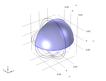
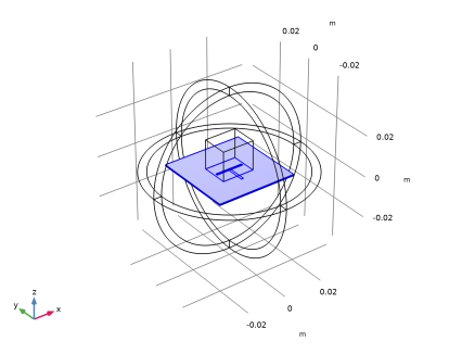
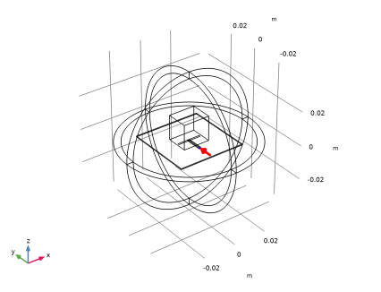
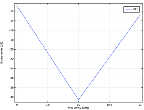
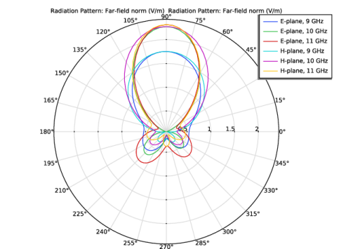
In the Model Builder window, expand the Results > 2D Far Field (emw) node, then click Radiation Pattern 1.
2
In the Settings window for Radiation Pattern, locate the Evaluation section.
3
Find the Angles subsection. In the Number of angles text field, type 100.
4
Find the Normal vector subsection. In the x text field, type 1.
5
In the z text field, type 0.
6
Find the Reference direction subsection. In the x text field, type 0.
7
In the y text field, type 1.
8
Click to expand the Legends section. From the Legends list, choose Manual.
9
10
In the 2D Far Field (emw) toolbar, click  Plot.
Radiation Pattern 2
1
Right-click Results > 2D Far Field (emw) > Radiation Pattern 1 and choose Duplicate.
2
In the Settings window for Radiation Pattern, locate the Evaluation section.
3
Find the Normal vector subsection. In the x text field, type 0.
4
In the y text field, type -1.
5
Find the Reference direction subsection. In the x text field, type 1.
6
In the y text field, type 0.
7
Locate the Legends section. In the table, enter the following settings:
8
In the 2D Far Field (emw) toolbar, click  Plot.
This is the far-field radiation patterns on the E-plane and H-plane (Figure 2).
3D Far Field, Gain (emw)
Compare the 3D far-field radiation pattern plot with Figure 3.