|
|
|
|
1
|
|
2
|
|
3
|
Click Add.
|
|
4
|
Click
|
|
5
|
|
6
|
Click
|
|
1
|
|
2
|
|
3
|
|
1
|
|
2
|
|
1
|
|
2
|
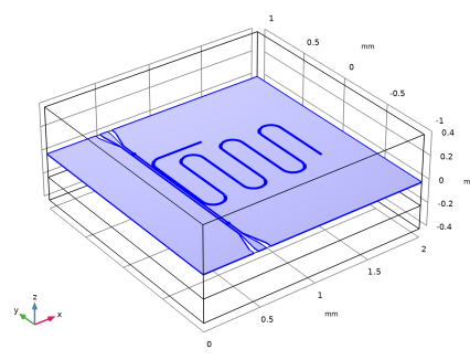
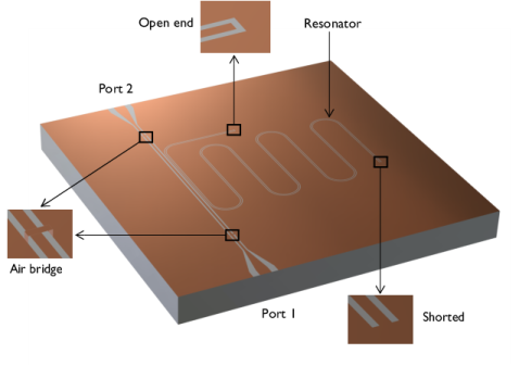
In the Part Libraries window, select RF Module > Coplanar Waveguides > cpw_straight_onchip in the tree.
|
|
3
|
Click
|
|
1
|
In the Model Builder window, under Component 1 (comp1) > Geometry 1 > Work Plane 1 (wp1) > Plane Geometry click Coplanar Waveguide Trace, Straight, On Chip 1 (pi1).
|
|
2
|
|
4
|
|
5
|
|
6
|
Click
|
|
1
|
|
2
|
In the Model Builder window, under Component 1 (comp1) > Geometry 1 > Work Plane 1 (wp1) click Plane Geometry.
|
|
3
|
In the Part Libraries window, select RF Module > Coplanar Waveguides > cpw_transition_onchip in the tree.
|
|
4
|
Click
|
|
1
|
In the Model Builder window, under Component 1 (comp1) > Geometry 1 > Work Plane 1 (wp1) > Plane Geometry click Coplanar Waveguide Trace, Transition, On Chip 1 (pi2).
|
|
2
|
|
4
|
Locate the Position and Orientation of Output section. In the xw-displacement text field, type 0.515.
|
|
5
|
|
6
|
|
7
|
Click
|
|
1
|
|
2
|
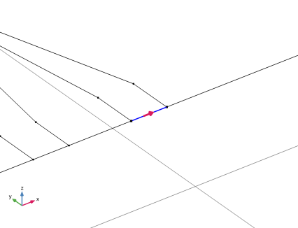
Select the object pi2 only.
|
|
3
|
|
4
|
|
5
|
|
6
|
Click
|
|
7
|
|
8
|
Click
|
|
9
|
|
1
|
In the Model Builder window, under Component 1 (comp1) > Geometry 1 > Work Plane 1 (wp1) > Plane Geometry right-click Coplanar Waveguide Trace, Straight, On Chip 1 (pi1) and choose Duplicate.
|
|
2
|
|
4
|
Locate the Position and Orientation of Output section. In the xw-displacement text field, type 0.834.
|
|
5
|
|
6
|
|
7
|
Click
|
|
1
|
Right-click Component 1 (comp1) > Geometry 1 > Work Plane 1 (wp1) > Plane Geometry > Coplanar Waveguide Trace, Straight, On Chip 2 (pi3) and choose Duplicate.
|
|
2
|
|
4
|
Locate the Position and Orientation of Output section. In the xw-displacement text field, type 0.5435.
|
|
5
|
|
6
|
|
7
|
Click
|
|
1
|
|
2
|
|
3
|
Select the object pi4 only.
|
|
4
|
|
5
|
|
6
|
|
7
|
Click
|
|
8
|
|
1
|
In the Model Builder window, under Component 1 (comp1) > Geometry 1 > Work Plane 1 (wp1) > Plane Geometry right-click Coplanar Waveguide Trace, Straight, On Chip 3 (pi4) and choose Duplicate.
|
|
2
|
|
4
|
|
5
|
Click
|
|
1
|
|
2
|
In the Model Builder window, under Component 1 (comp1) > Geometry 1 > Work Plane 1 (wp1) click Plane Geometry.
|
|
3
|
In the Part Libraries window, select RF Module > Coplanar Waveguides > cpw_90_round_bend_onchip in the tree.
|
|
4
|
Click
|
|
1
|
In the Model Builder window, under Component 1 (comp1) > Geometry 1 > Work Plane 1 (wp1) > Plane Geometry click Coplanar Waveguide Trace, 90-Degree Round-Bend, On Chip 1 (pi6).
|
|
2
|
|
4
|
Locate the Position and Orientation of Output section. In the xw-displacement text field, type 0.636.
|
|
5
|
|
6
|
|
7
|
Click
|
|
1
|
|
2
|
In the Model Builder window, under Component 1 (comp1) > Geometry 1 > Work Plane 1 (wp1) click Plane Geometry.
|
|
3
|
In the Part Libraries window, select RF Module > Coplanar Waveguides > cpw_180_round_bend_onchip in the tree.
|
|
4
|
Click
|
|
1
|
In the Model Builder window, under Component 1 (comp1) > Geometry 1 > Work Plane 1 (wp1) > Plane Geometry click Coplanar Waveguide Trace, 180-Degree Round-Bend, On Chip 1 (pi7).
|
|
2
|
|
4
|
Locate the Position and Orientation of Output section. In the xw-displacement text field, type 0.636.
|
|
5
|
|
6
|
|
7
|
Click
|
|
1
|
|
2
|
|
3
|
Select the object pi7 only.
|
|
4
|
|
5
|
|
6
|
|
7
|
Click
|
|
1
|
|
2
|
|
3
|
|
4
|
Select the Keep input objects checkbox.
|
|
5
|
|
6
|
|
7
|
Click
|
|
1
|
In the Model Builder window, under Component 1 (comp1) > Geometry 1 > Work Plane 1 (wp1) > Plane Geometry right-click Coplanar Waveguide Trace, Straight, On Chip 3 (pi4) and choose Duplicate.
|
|
2
|
|
4
|
Locate the Position and Orientation of Output section. In the xw-displacement text field, type 1.6535.
|
|
5
|
Click
|
|
1
|
|
2
|
|
3
|
|
4
|
|
5
|
|
6
|
|
7
|
|
8
|
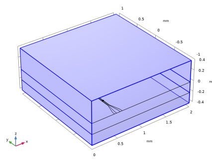
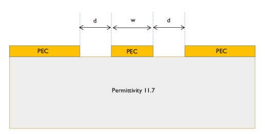
Click to expand the Layers section. In the table, enter the following settings:
|
|
9
|
Click
|
|
1
|
|
2
|
|
3
|
|
4
|
|
5
|
|
6
|
|
7
|
|
8
|
|
9
|
|
10
|
|
11
|
Click
|
|
1
|
|
2
|
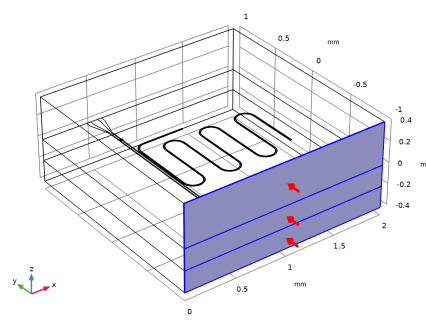
Select the object blk2 only.
|
|
3
|
|
4
|
|
5
|
|
6
|
|
7
|
Click
|
|
1
|
|
1
|
|
1
|
|
3
|
|
4
|
|
5
|
Select the Analyze as a TEM field checkbox.
|
|
1
|
|
2
|
|
3
|
Click
|
|
1
|
|
3
|
|
4
|
|
5
|
Select the Analyze as a TEM field checkbox.
|
|
1
|
|
2
|
|
3
|
Click
|
|
5
|
|
1
|
|
2
|
Go to the Add Material window.
|
|
3
|
|
4
|
Click the Add to Component button in the window toolbar.
|
|
5
|
|
6
|
Click the Add to Component button in the window toolbar.
|
|
7
|
|
1
|
|
2
|
|
3
|
Select the Refine conductive edges checkbox.
|
|
4
|
|
5
|
|
6
|
|
1
|
|
2
|
|
3
|
|
4
|
|
1
|
|
2
|
|
3
|
|
4
|
|
1
|
|
2
|
|
3
|
|
1
|
|
2
|
|
3
|
|
4
|
|
5
|
|
1
|
|
2
|
|
3
|
In the Model Builder window, expand the Study 1 > Solver Configurations > Solution 1 (sol1) > Eigenvalue Solver 3 node.
|
|
4
|
Right-click Study 1 > Solver Configurations > Solution 1 (sol1) > Eigenvalue Solver 3 > Suggested Iterative Solver (emw) 2 and choose Enable.
|
|
5
|
|
1
|
|
2
|
|
3
|
|
4
|
|
5
|
|
1
|
|
2
|
|
3
|
|
4
|
|
5
|
|
6
|
|
1
|
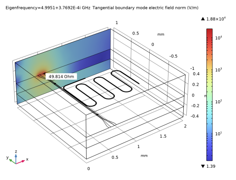
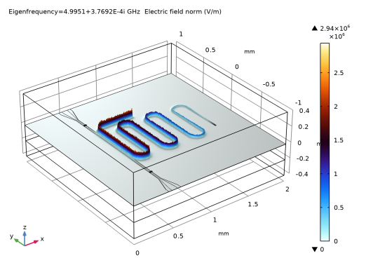
In the Model Builder window, expand the Electric Mode Field, Port 2 (emw) node, then click Surface 1.
|
|
2
|
|
3
|
|
1
|
|
2
|
Go to the Add Study window.
|
|
3
|
|
4
|
Click the Add Study button in the window toolbar.
|
|
5
|
|
1
|
|
2
|
|
3
|
Clear the Generate default plots checkbox.
|
|
1
|
In the Study toolbar, click
|
|
2
|
|
3
|
|
5
|
Click to expand the Store in Output section. In the table, enter the following settings:
|
|
6
|
|
1
|
|
2
|
|
3
|
|
1
|
|
2
|
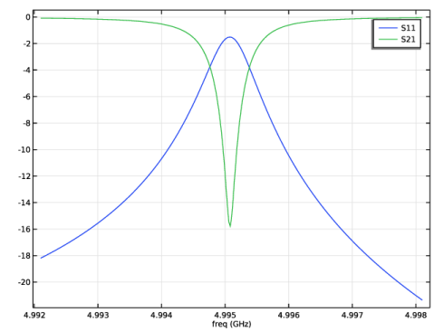
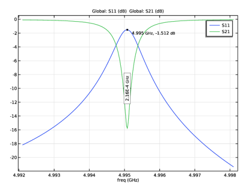
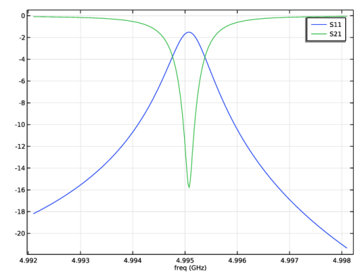
In the Settings window for Global, click Replace Expression in the upper-right corner of the y-Axis Data section. From the menu, choose Component 1 (comp1) > Electromagnetic Waves, Frequency Domain > Ports > S-parameter, dB - dB > emw.S11dB - S11.
|
|
3
|
Click Add Expression in the upper-right corner of the y-Axis Data section. From the menu, choose Component 1 (comp1) > Electromagnetic Waves, Frequency Domain > Ports > S-parameter, dB - dB > emw.S21dB - S21.
|
|
4
|
|
1
|
|
2
|
In the Settings window for 1D Plot Group, type S-parameter with Graph Markers in the Label text field.
|
|
3
|
|
1
|
|
2
|
In the Settings window for Global, click Replace Expression in the upper-right corner of the y-Axis Data section. From the menu, choose Component 1 (comp1) > Electromagnetic Waves, Frequency Domain > Ports > S-parameter, dB - dB > emw.S11dB - S11.
|
|
1
|
|
2
|
|
3
|
|
4
|
|
5
|
Select the Show x-coordinate checkbox.
|
|
6
|
Select the Include unit checkbox.
|
|
7
|
|
1
|
|
2
|
In the Settings window for Global, click Replace Expression in the upper-right corner of the y-Axis Data section. From the menu, choose Component 1 (comp1) > Electromagnetic Waves, Frequency Domain > Ports > S-parameter, dB - dB > emw.S21dB - S21.
|
|
1
|
|
2
|
|
3
|
|
4
|
|
5
|
|
6
|
|
7
|
Select the Include unit checkbox.
|
|
8
|
|
9
|
Select the Show frame checkbox.
|
|
10
|