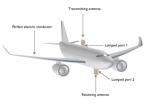
PDF

Simulating Antenna Crosstalk on an Airplane’s Fuselage
Introduction
Antenna crosstalk, or co-site interference, is problematic when multiple antennas are used on a single large platform. In this example, the interference between two identical antennas at VHF frequency is studied with an S-parameter analysis of different configurations of a receiving antenna installed on an airplane fuselage. The 2D and 3D far-field radiation patterns of a transmitting antenna are computed and the lit and shadow areas on the airplane surface are also visualized.
Figure 1: An airplane with ~20 m length of fuselage is simply depicted as an all-metallic structure except for the antenna enclosure. The surrounding air domain and perfectly matched layers are not shown.
Model Definition
The airplane is composed of two parts: a simplified metallic body and two antennas on its fuselage. All metal surfaces are modeled as perfect electric conductor (PEC). The PEC condition is automatically applied to all exterior boundaries. Removing the airplane body causes its surfaces to become effectively exterior and the PEC condition is applied by default. The antenna is made out of very thin metal strips inserted inside a dielectric (εr = 4.3) block. The antenna is miniaturized with a meander line design, which decreases the antenna input impedance. To match the initial low input impedance with regard to conventional 50 Ω, a folded monopole antenna (effectively a folded dipole) on a large ground plane method is used.
The entire airplane is enclosed by a spherical air domain which is finished with perfectly matched layers on the outermost parts. This mimics the antenna testing in infinite free space without causing unwanted reflection from the outer walls.
On each antenna, a lumped port is assigned on the gap between the metallic meander line and the airplane’s fuselage. S-parameters are calculated from two lumped ports that show the antenna matching properties as well as the amount of interference in the given configuration.
The receiving antenna is located at three difference places on the bottom side of the fuselage, and this location variation is modeled using a parametric sweep.
Results and Discussion
Figure 2 shows the E-field norm distribution in dB scale on a vertical cut plane at each location of the receiving antenna. Regardless of the location, the antenna on the bottom side of the fuselage is reacting to the field from the transmitting antenna on the top of the fuselage, so there is no complete shadow region with any of these three locations.
To identify lit and shadow areas, the E-field norm is visualized on the airplane surface in Figure 3. By adjusting the display color range, the difference between the two categories is emphasized. The areas around turbines, rear wings, and some regions of the bottom side of the main wings and fuselage are relatively less affected by the transmitting antenna.
See Figure 4 where the E-field norm is plotted in dB scale while the receiving antenna on the fuselage bottom is moved from the rear to the front side. From the XY view, the shadow area is visible, located at the rear end of the fuselage bottom.
The amount of interference can be also quantitatively described in terms of S-parameters (Table 1) and the computed S21 gives a more clear clue about where to install the second antenna to minimize the crosstalk to the first antenna.
Figure 2: E-field norm plot in dB scale on the yz-plane with the receiving antenna at locations on the fuselage bottom from the rear to front side.
Figure 3: E-field norm on the airplane surface. The visualization color range is adjusted to emphasize the lit and shadow regions due to the transmitting antenna.
Table 1: S-parameters.
S11
S21
Figure 4: E-field norm plot in dB scale from the XY view with the receiving antenna on the fuselage bottom from the rear to front side. The shadow area is located on the rear side.
Application Library path: RF_Module/EMI_EMC_Applications/airplane_antenna_crosstalk
Modeling Instructions
From the File menu, choose New.
New
In the New window, click  Model Wizard.
Model Wizard
1
In the Model Wizard window, click  3D.
2
In the Select Physics tree, select Radio Frequency > Electromagnetic Waves, Frequency Domain (emw).
3
Click Add.
4
Click  Study.
5
In the Select Study tree, select General Studies > Frequency Domain.
6
Study 1
Step 1: Frequency Domain
Define the study frequency ahead of performing any frequency-dependent operation such as building mesh. The physics-controlled mesh uses the specified frequency value.
1
In the Model Builder window, under Study 1 click Step 1: Frequency Domain.
2
In the Settings window for Frequency Domain, locate the Study Settings section.
3
In the Frequencies text field, type 30[MHz].
Global Definitions
Parameters 1
1
In the Model Builder window, under Global Definitions click Parameters 1.
2
In the Settings window for Parameters, locate the Parameters section.
3
Geometry 1
Import 1 (imp1)
1
In the Geometry toolbar, click  Import.
2
In the Settings window for Import, locate the Source section.
3
Click  Browse.
4
5
Click  Import.
Import 2 (imp2)
1
In the Geometry toolbar, click  Import.
2
In the Settings window for Import, locate the Source section.
3
Click  Browse.
4
5
Click  Import.
6
Click the  Wireframe Rendering button in the Graphics toolbar.
Mirror 1 (mir1)
1
In the Geometry toolbar, click  Transforms and choose Mirror.
2
3
In the Settings window for Mirror, locate the Input section.
4
Select the Keep input objects checkbox.
Move 1 (mov1)
1
In the Geometry toolbar, click  Transforms and choose Move.
2
3
In the Settings window for Move, locate the Displacement section.
4
In the y text field, type a_y.
Sphere 1 (sph1)
1
In the Geometry toolbar, click  Sphere.
2
In the Settings window for Sphere, locate the Size section.
3
In the Radius text field, type 13.
4
Click to expand the Layers section. In the table, enter the following settings:
A perfectly matched layer (PML) will be configured in this layer. A PML with a thickness of approximately 0.1 wavelengths works well for an incident wave that is normal to the surface.
Difference 1 (dif1)
1
In the Geometry toolbar, click  Booleans and Partitions and choose Difference.
2
Select the objects imp2, mov1, and sph1 only.
3
In the Settings window for Difference, locate the Difference section.
4
Click to select the  Activate Selection toggle button for Objects to subtract.
5
6
Select the Keep objects to subtract checkbox.
7
Click  Build All Objects.
Disable the analysis of the geometry as the remaining small geometric details can be kept.
8
In the Model Builder window, click Geometry 1.
9
In the Settings window for Geometry, locate the Cleanup section.
10
Clear the Automatic detection of small details checkbox.
Definitions
Perfectly Matched Layer 1 (pml1)
1
In the Definitions toolbar, click  Perfectly Matched Layer.
2
3
In the Settings window for Perfectly Matched Layer, locate the Geometry section.
4
From the Type list, choose Spherical.
Explicit 1
1
In the Definitions toolbar, click  Explicit.
2
3
In the Settings window for Explicit, locate the Output Entities section.
4
From the Output entities list, choose Adjacent boundaries.
Electromagnetic Waves, Frequency Domain (emw)
Perfect Electric Conductor 2
1
In the Physics toolbar, click  Boundaries and choose Perfect Electric Conductor.
2
Click the  Zoom In button in the Graphics toolbar.
3
Perfect Electric Conductor 3
1
In the Physics toolbar, click  Domains and choose Perfect Electric Conductor.
2
Lumped Port 1
1
In the Physics toolbar, click  Boundaries and choose Lumped Port.
2
For the first port, wave excitation is on by default.
Lumped Port 2
1
In the Physics toolbar, click  Boundaries and choose Lumped Port.
2
Far-Field Domain 1
In the Physics toolbar, click  Domains and choose Far-Field Domain.
Add Material
1
In the Materials toolbar, click  Add Material to open the Add Material window.
2
Go to the Add Material window.
3
In the tree, select Built-in > Air.
4
Click the Add to Component button in the window toolbar.
5
In the Materials toolbar, click  Add Material to close the Add Material window.
Materials
Material 2 (mat2)
1
In the Model Builder window, under Component 1 (comp1) right-click Materials and choose Blank Material.
2
3
In the Settings window for Material, locate the Material Contents section.
4
Mesh 1
1
In the Model Builder window, under Component 1 (comp1) click Mesh 1.
2
In the Settings window for Mesh, locate the Physics-Controlled Mesh section.
3
From the Element size list, choose Coarse.
4
Locate the Electromagnetic Waves, Frequency Domain (emw) section. Select the Refine conductive edges checkbox.
Information 1
1
In the Mesh toolbar, click  Build Mesh.
2
Click the  Zoom Out button in the Graphics toolbar.
Definitions
Hide for Physics 1
1
In the Model Builder window, right-click View 1 and choose Hide for Physics.
2
In the Settings window for Hide for Physics, locate the Geometric Entity Selection section.
3
From the Geometric entity level list, choose Boundary.
4
Click  Paste Selection.
5
In the Paste Selection dialog, type 6, 10, 108, 115, 124, 127, 129 in the Selection text field.
6
Mesh 1
In the Model Builder window, under Component 1 (comp1) click Mesh 1.
Study 1
Parametric Sweep
1
In the Study toolbar, click  Parametric Sweep.
2
In the Settings window for Parametric Sweep, locate the Study Settings section.
3
4
With this parameter, the receiving antenna on the fuselage bottom is relocated in this order: front, middle, and rear position.
Step 1: Frequency Domain
In the Study toolbar, click  Compute.
Results
Multislice 1
1
In the Model Builder window, expand the Electric Field (emw) node, then click Multislice 1.
2
In the Settings window for Multislice, locate the Multiplane Data section.
3
Find the Y-planes subsection. In the Planes text field, type 0.
4
Find the Z-planes subsection. In the Planes text field, type 0.
5
Locate the Expression section. In the Expression text field, type 20*log10(emw.normE).
6
Click to expand the Range section. Select the Manual color range checkbox.
7
In the Minimum text field, type -50.
8
In the Maximum text field, type 50.
9
In the Electric Field (emw) toolbar, click  Plot.
10
Click the  Zoom In button in the Graphics toolbar.
Electric Field (emw)
1
In the Model Builder window, click Electric Field (emw).
2
In the Settings window for 3D Plot Group, locate the Data section.
3
From the Parameter value (a_y (m)) list, choose -2.
4
In the Electric Field (emw) toolbar, click  Plot.
5
From the Parameter value (a_y (m)) list, choose -5.
6
In the Electric Field (emw) toolbar, click  Plot.
Compare the plot for each different location of the receiving antenna with Figure 2.
S-Parameter (emw)
In the Model Builder window, click S-Parameter (emw).
Reflection Graph 1
1
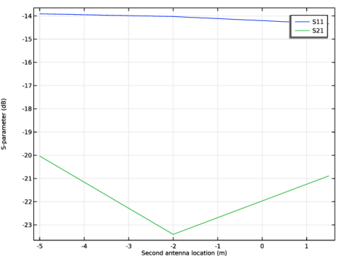
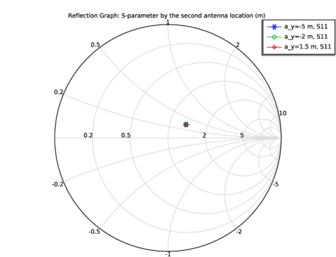
In the Model Builder window, expand the Results > Smith Plot (emw) node, then click Reflection Graph 1.
2
In the Settings window for Reflection Graph, click to expand the Title section.
3
In the Title text area, type Reflection Graph: S-parameter by the second antenna location (m).
4
Click to expand the Coloring and Style section. Find the Line markers subsection. From the Marker list, choose Cycle.
5
From the Positioning list, choose Interpolated.
Color Expression 1
1
In the Model Builder window, expand the Reflection Graph 1 node.
2
Right-click Color Expression 1 and choose Delete.
Reflection Graph 1
Multislice 1
1
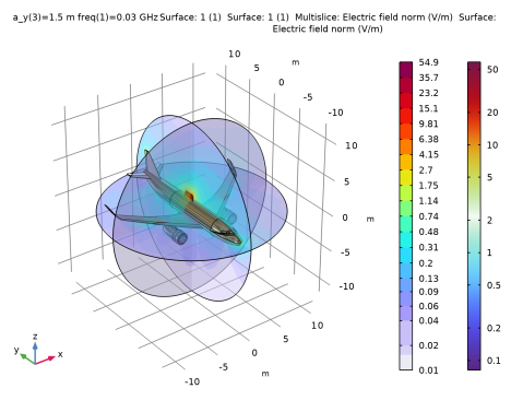
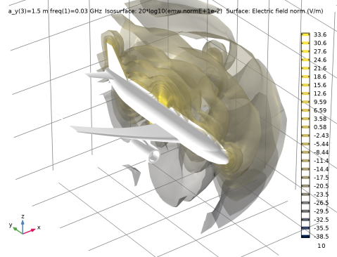
In the Model Builder window, expand the Results > Electric Field, Logarithmic (emw) node, then click Multislice 1.
2
In the Settings window for Multislice, click to expand the Range section.
3
Select the Manual color range checkbox.
4
In the Minimum text field, type 0.01.
5
In the Electric Field, Logarithmic (emw) toolbar, click  Plot.
Radiation Pattern 1
1
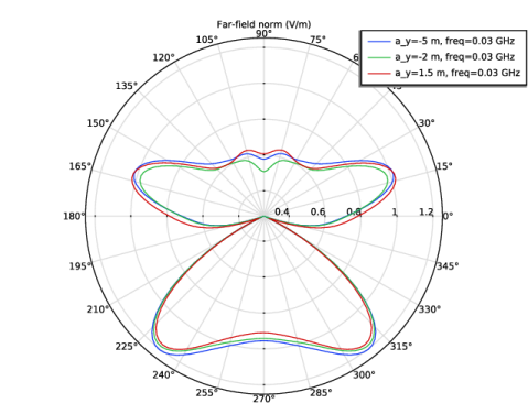
In the Model Builder window, expand the Results > 2D Far Field (emw) node, then click Radiation Pattern 1.
2
In the 2D Far Field (emw) toolbar, click  Plot.
Radiation Pattern 1
1
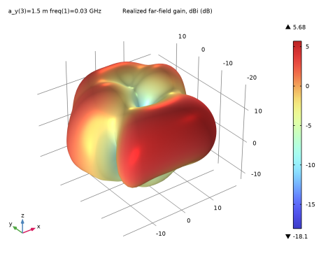
In the Model Builder window, expand the Results > 3D Far Field, Gain (emw) node, then click Radiation Pattern 1.
2
In the Settings window for Radiation Pattern, locate the Evaluation section.
3
Find the Angles subsection. In the Number of elevation angles text field, type 90.
4
In the Number of azimuth angles text field, type 90.
5
In the 3D Far Field, Gain (emw) toolbar, click  Plot.
Electric Field on Surface
1
In the Results toolbar, click  3D Plot Group.
2
In the Settings window for 3D Plot Group, type Electric Field on Surface in the Label text field.
3
Locate the Data section. From the Dataset list, choose Study 1/Parametric Solutions 1 (sol2).
4
Locate the Plot Settings section. Clear the Plot dataset edges checkbox.
Surface 1
Right-click Electric Field on Surface and choose Surface.
Selection 1
1
In the Model Builder window, right-click Surface 1 and choose Selection.
2
In the Settings window for Selection, locate the Selection section.
3
From the Selection list, choose Explicit 1.
Surface 1
1
In the Model Builder window, click Surface 1.
2
In the Settings window for Surface, locate the Expression section.
3
In the Expression text field, type 20*log10(emw.normE+1e-3).
4
Click to expand the Range section. Select the Manual color range checkbox.
5
In the Minimum text field, type -30.
6
In the Maximum text field, type 0.
7
Locate the Coloring and Style section. From the Color table list, choose Dipole.
8
In the Electric Field on Surface toolbar, click  Plot.
See Figure 3 to compare the reproduced plot.
S-Parameter (emw)
The S11 value should be below -10 dB for all three antenna locations.
Based on the S21 values, the best location for the least interference can be identified.
Surface 1
Click the  Zoom In button in the Graphics toolbar, a couple of times to get a view of the fuselage bottom.
Electric Field on Surface
1
In the Model Builder window, click Electric Field on Surface.
2
In the Settings window for 3D Plot Group, locate the Data section.
3
From the Parameter value (a_y (m)) list, choose -2.
4
In the Electric Field on Surface toolbar, click  Plot.
5
From the Parameter value (a_y (m)) list, choose -5.
6
In the Electric Field on Surface toolbar, click  Plot.
The cold spot for the least interference can be identified from the plot shown in Figure 4.
Electric Field in Air Domain
1
In the Results toolbar, click  3D Plot Group.
2
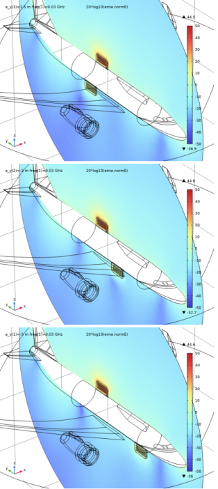
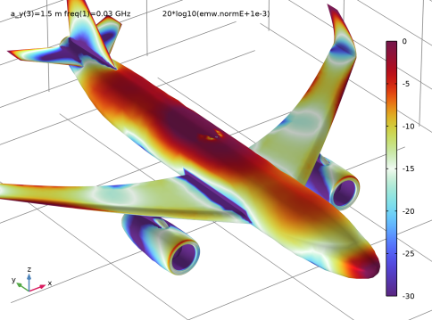
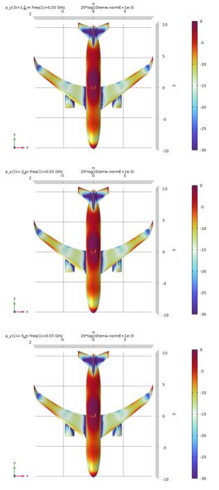
In the Settings window for 3D Plot Group, type Electric Field in Air Domain in the Label text field.
3
Locate the Data section. From the Dataset list, choose Study 1/Parametric Solutions 1 (sol2).
4
Locate the Plot Settings section. Clear the Plot dataset edges checkbox.
Isosurface 1
1
Right-click Electric Field in Air Domain and choose Isosurface.
2
In the Settings window for Isosurface, locate the Expression section.
3
In the Expression text field, type 20*log10(emw.normE+1e-2).
4
Locate the Levels section. In the Total levels text field, type 25.
5
Locate the Coloring and Style section. From the Color table list, choose Cividis.
The color table Cividis is optimized for viewing scalar data. The color table benefits people both with and without color vision deficiency.
6
From the Color table transformation list, choose Nonlinear.
7
Set the Color calibration parameter value to -1.5.
Filter 1
1
Right-click Isosurface 1 and choose Filter.
2
In the Settings window for Filter, locate the Element Selection section.
3
In the Logical expression for inclusion text field, type x>0.
Selection 1
1
In the Model Builder window, right-click Isosurface 1 and choose Selection.
2
3
Click the  Go to Default View button in the Graphics toolbar.
Transparency 1
1
Right-click Isosurface 1 and choose Transparency.
2
Click the  Zoom In button in the Graphics toolbar.
Surface 1
In the Model Builder window, right-click Electric Field in Air Domain and choose Surface.
Selection 1
1
In the Model Builder window, right-click Surface 1 and choose Selection.
2
In the Settings window for Selection, locate the Selection section.
3
From the Selection list, choose Explicit 1.
Material Appearance 1
1
In the Model Builder window, right-click Surface 1 and choose Material Appearance.
2
In the Settings window for Material Appearance, locate the Appearance section.
3
From the Appearance list, choose Custom.
4
From the Material type list, choose Plastic (shiny).
5
In the Electric Field in Air Domain toolbar, click  Plot.