PDF

Thin-Film Resistance
Introduction
When modeling transport by diffusion or conduction in thin layers, large differences in dimensions of the different domains are common. If the model has a sandwich structure, you can replace the thinnest layers with a thin-layer approximation, provided that the difference in thickness is large.
Model Definition
This study explains the principle of the thin-layer approximation in direct current conduction problems. A comparison of a structure with three domains to a simplified model that replaces the domain in the middle with a thin-layer approximation shows the benefit of this approach (see Figure 1).
Figure 1: Exact domain description (left) and approximation (right). The current flows from the base plate to the circular plate on the upper surface of the device.
Equation 1 below describes the current balance in all three domains in the real sandwich structure:
(1)
In this equation, σ represents the conductivity and V the electric potential. In this case, there is a substantial difference in conductivity between the thin and thicker layers of the structure. The boundary conditions include a current inlet in the base plate of the device and a constant potential at the upper circular boundary (see Figure 1). All other boundaries are insulated.
The simplified model is based on the assumption that the components of the current density vector in the x and y directions are small and that the dominating transport through the thin structure is obtained in the z direction. For the middle layer, this implies that you can approximate Equation 1 by the one-dimensional equation
(2)
It is possible to solve this equation analytically if the potential is given at the lower and upper surfaces of the middle layer:
(3)
(4)
You can integrate Equation 2 analytically to give:
where a and b are integration constants. If you arbitrarily place z = 0 at the lower boundary of the middle layer, you get the constants a and b from the boundary conditions in Equation 3 and Equation 4:
This gives:
The resulting equation for the potential is thus
(5)
The current density is defined as
(6)
Combining Equation 5 and Equation 6 gives
(7)
In the thin-film approximation the potential is discontinuous at the film boundary. Use the Contact Impedance node on interior boundaries to model a thin layer of resistive material.
It is also possible to derive the expression for the current density in Equation 7 by approximating the gradient using the potential difference over the thin layer. This example includes the previous tedious derivation to show that this is exactly what you obtain from the solution of Equation 2.
The approximation presented in this example is not limited to direct current problems. You can also use it for modeling of diffusion, heat conduction, flow through porous media using Darcy’s law, and other types of physics that the divergence of a gradient flux describes.
In general, the application of this simplification is appropriate in cases where the differences in thickness are so large that the mesh generator cannot even mesh the domain. In some cases, the mesh generator might be able to mesh the domain but then creates a very large number of elements.
Results and Discussion
Figure 2 shows a comparison between the exact solution of the problem using three conductive layers and the thin-film approximation. The comparison reveals an excellent agreement in the potential and current distribution despite that the middle film in this study is relatively thick. The approximation becomes even more accurate as the film thickness between the upper and lower domain decreases.
Figure 2: Potential distribution in the modeled device. The value of the potential loss over the device at a current of 0.3 A is almost identical in the two models: the full model (left) and thin-film approximation (right).
Figure 3 shows a cross-section plot of the potential through the structure’s center for the full model and for the approximation. The plots show the excellent agreement obtained between the two models.
Figure 3: Potential distribution along the z direction in the middle of the device. Solution for the full model (blue line) and for the thin-film approximation (green line).
Application Library path: COMSOL_Multiphysics/Electromagnetics/thin_film_resistance
Modeling Instructions
From the File menu, choose New.
New
In the New window, click  Model Wizard.
Model Wizard
1
In the Model Wizard window, click  3D.
2
In the Select Physics tree, select AC/DC > Electric Fields and Currents > Electric Currents (ec).
3
Click Add.
4
Click  Study.
5
In the Select Study tree, select General Studies > Stationary.
6
Geometry 1
Work Plane 1 (wp1)
1
In the Geometry toolbar, click  Work Plane.
2
In the Settings window for Work Plane, locate the Plane Definition section.
3
In the z-coordinate text field, type 0.1.
4
Locate the Unite Objects section. Clear the Unite objects checkbox.
5
Click  Go to Plane Geometry.
Work Plane 1 (wp1) > Circle 1 (c1)
1
In the Work Plane toolbar, click  Circle.
2
In the Settings window for Circle, locate the Size and Shape section.
3
In the Radius text field, type 0.6.
4
Locate the Position section. In the yw text field, type 1.
5
In the Work Plane toolbar, click  Build All.
Work Plane 1 (wp1) > Square 1 (sq1)
1
In the Work Plane toolbar, click  Square.
2
Click  Build All.
3
Click the  Zoom Extents button in the Graphics toolbar.
Work Plane 1 (wp1) > Intersection 1 (int1)
1
In the Work Plane toolbar, click  Booleans and Partitions and choose Intersection.
2
Click in the Graphics window and then press Ctrl+A to select both objects.
3
In the Work Plane toolbar, click  Build All.
Work Plane 1 (wp1) > Square 2 (sq2)
1
In the Work Plane toolbar, click  Square.
2
Click  Build All.
3
Click the  Zoom Extents button in the Graphics toolbar.
The 2D geometry should now look as in the figure below.
Extrude 1 (ext1)
1
In the Model Builder window, under Component 1 (comp1) > Geometry 1 right-click Work Plane 1 (wp1) and choose Extrude.
2
Select the object wp1.sq2 only.
3
In the Settings window for Extrude, locate the Distances section.
4
Block 1 (blk1)
1
In the Geometry toolbar, click  Block.
2
In the Settings window for Block, locate the Size and Shape section.
3
In the Height text field, type 0.1.
4
Locate the Position section. In the z text field, type -0.1.
Copy the above geometry and build the geometry for the full 3D model.
Copy 1 (copy1)
1
In the Geometry toolbar, click  Transforms and choose Copy.
2
Click in the Graphics window and then press Ctrl+A to select all objects.
3
In the Settings window for Copy, locate the Displacement section.
4
In the x text field, type 1.5.
5
In the y text field, type -1.
Move 1 (mov1)
1
In the Geometry toolbar, click  Transforms and choose Move.
2
3
In the Settings window for Move, locate the Displacement section.
4
In the z text field, type -0.02.
Block 2 (blk2)
1
In the Geometry toolbar, click  Block.
2
In the Settings window for Block, locate the Size and Shape section.
3
In the Height text field, type 0.02.
4
Locate the Position section. In the z text field, type -0.02.
5
Click  Build All Objects.
6
Click the  Zoom Extents button in the Graphics toolbar.
The geometry for the Thin-Film Approximation and the Full 3D model should look as in the figure below.
Electric Currents (ec)
Current Conservation in Solids 1
1
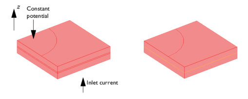
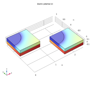
In the Model Builder window, under Component 1 (comp1) > Electric Currents (ec) click Current Conservation in Solids 1.
2
In the Settings window for Current Conservation in Solids, locate the Constitutive Relation Jc-E section.
3
From the σ list, choose User defined. In the associated text field, type 1.
4
Locate the Constitutive Relation D-E section. From the εr list, choose User defined.
Normal Current Density 1
1
In the Physics toolbar, click  Boundaries and choose Normal Current Density.
2
3
In the Settings window for Normal Current Density, locate the Normal Current Density section.
4
In the Jn text field, type 0.3.
Ground 1
1
In the Physics toolbar, click  Boundaries and choose Ground.
2
Contact Impedance 1
1
In the Physics toolbar, click  Boundaries and choose Contact Impedance.
2
Click the  Wireframe Rendering button in the Graphics toolbar.
3
4
Click the  Wireframe Rendering button in the Graphics toolbar to restore the rendering setting.
5
In the Settings window for Contact Impedance, locate the Contact Impedance section.
6
In the ds text field, type 0.02.
7
From the σ list, choose User defined. Keep the default value.
8
From the εr list, choose User defined. Again, the default value applies.
Current Conservation in Solids 2
1
In the Physics toolbar, click  Domains and choose Current Conservation in Solids.
2
3
In the Settings window for Current Conservation in Solids, locate the Constitutive Relation Jc-E section.
4
From the σ list, choose User defined. In the associated text field, type 0.01.
5
Locate the Constitutive Relation D-E section. From the εr list, choose User defined.
Mesh 1
1
In the Model Builder window, under Component 1 (comp1) click Mesh 1.
2
In the Settings window for Mesh, locate the Physics-Controlled Mesh section.
3
From the Element size list, choose Coarse.
Study 1
1
In the Model Builder window, click Study 1.
2
In the Settings window for Study, locate the Study Settings section.
3
Clear the Generate default plots checkbox, because you will add the desired plots manually.
4
In the Study toolbar, click  Compute.
Results
The following steps show you how to reproduce the volume plot of the potential (Figure 2).
3D Plot Group 1
In the Results toolbar, click  3D Plot Group.
Volume 1
1
Right-click 3D Plot Group 1 and choose Volume.
2
In the Settings window for Volume, locate the Coloring and Style section.
3
Clear the Color legend checkbox.
4
From the Color table list, choose RainbowLight.
5
In the 3D Plot Group 1 toolbar, click  Plot.
Follow the steps below to visualize the potential distribution along the z direction in the middle of the device (Figure 3).
Cut Line 3D 1
1
In the Results toolbar, click  Cut Line 3D.
2
In the Settings window for Cut Line 3D, locate the Line Data section.
3
In row Point 1, set x to 0.5, y to 0.5, and z to -0.1.
4
In row Point 2, set x to 0.5, y to 0.5, and z to 0.1.
Cut Line 3D 2
1
Right-click Cut Line 3D 1 and choose Duplicate.
2
In the Settings window for Cut Line 3D, locate the Line Data section.
3
In row Point 1, set x to 2.
4
In row Point 1, set y to -0.5.
5
In row Point 2, set x to 2.
6
In row Point 2, set y to -0.5.
1D Plot Group 2
1
In the Results toolbar, click  1D Plot Group.
2
In the Settings window for 1D Plot Group, click to expand the Title section.
3
From the Title type list, choose None.
4
Locate the Axis section. Select the Manual axis limits checkbox.
5
In the x minimum text field, type -0.1.
6
In the x maximum text field, type 0.1.
7
In the y minimum text field, type 0.2.
Line Graph 1
1
Right-click 1D Plot Group 2 and choose Line Graph.
2
In the Settings window for Line Graph, locate the Data section.
3
From the Dataset list, choose Cut Line 3D 1.
4
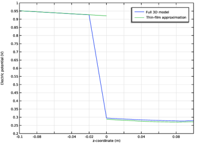
Click Replace Expression in the upper-right corner of the x-Axis Data section. From the menu, choose Component 1 (comp1) > Geometry > Coordinate > z - z-coordinate.
5
Click to expand the Legends section. Select the Show legends checkbox.
6
From the Legends list, choose Manual.
7
Line Graph 2
1
Right-click Line Graph 1 and choose Duplicate.
2
In the Settings window for Line Graph, locate the Data section.
3
From the Dataset list, choose Cut Line 3D 2.
4
Locate the Legends section. In the table, enter the following settings:
5
In the 1D Plot Group 2 toolbar, click  Plot.