|
|
|


|
1
|
|
2
|
|
3
|
Click Add.
|
|
4
|
Click
|
|
5
|
|
6
|
Click
|
|
1
|
|
2
|
|
1
|
In the Model Builder window, expand the Component 1 (comp1) > Geometry 1 node, then click Geometry 1.
|
|
2
|
|
3
|
|
4
|
|
1
|
|
2
|
|
3
|
|
4
|
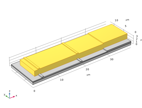
Browse to the model’s Application Libraries folder and double-click the file biased_resonator_3d_ecad_design_layout.gds.
|
|
5
|
|
7
|
Click to expand the Selections of Resulting Entities section. Find the Cumulative selection subsection. Click New.
|
|
8
|
|
9
|
Click OK.
|
|
10
|
|
1
|
|
2
|
In the Settings window for Import, type Import 2 = L2, Deposit Nitride Layer in the Label text field.
|
|
3
|
Locate the Layers section. In the table, enter the following settings:
|
|
4
|
Click to expand the Selections of Resulting Entities section. Find the Cumulative selection subsection. Click New.
|
|
5
|
|
6
|
Click OK.
|
|
7
|
|
8
|
|
1
|
|
2
|
In the Settings window for Import, type Import 3 = L3, Deposit and Pattern Base Layer in the Label text field.
|
|
3
|
Locate the Layers section. In the table, enter the following settings:
|
|
4
|
Click to expand the Selections of Resulting Entities section. Find the Cumulative selection subsection. Click New.
|
|
5
|
|
6
|
Click OK.
|
|
7
|
|
1
|
|
2
|
In the Settings window for Import, type Import 4 = L4, Deposit and Pattern Bottom Electrode Layer in the Label text field.
|
|
3
|
Locate the Layers section. In the table, enter the following settings:
|
|
4
|
Click to expand the Selections of Resulting Entities section. Find the Cumulative selection subsection. Click New.
|
|
5
|
|
6
|
Click OK.
|
|
7
|
|
1
|
|
2
|
|
3
|
|
4
|
|
5
|
In the Add dialog, in the Selections to add list, choose LAYER20 (Import 2 = L2, Deposit Nitride Layer), LAYER31 (Import 3 = L3, Deposit and Pattern Base Layer), and LAYER32 (Import 4 = L4, Deposit and Pattern Bottom Electrode Layer).
|
|
6
|
Click OK.
|
|
1
|
|
2
|
|
3
|
|
4
|
Select the Keep input objects checkbox.
|
|
5
|
Clear the Keep interior boundaries checkbox.
|
|
6
|
Locate the Selections of Resulting Entities section. Select the Resulting objects selection checkbox.
|
|
1
|
|
2
|
|
3
|
|
4
|
|
5
|
Click
|
|
6
|
|
7
|
Click OK.
|
|
8
|
|
9
|
|
10
|
|
11
|
|
12
|
|
13
|
|
1
|
|
2
|
In the Settings window for Offset Faces, type Offset Faces 1 - Deposit Sacrificial Layer in the Label text field.
|
|
3
|
|
4
|
Select the Subtract input objects checkbox.
|
|
5
|
|
6
|
Locate the Selections of Resulting Entities section. Select the Resulting objects selection checkbox.
|
|
7
|
|
8
|
Locate the Selections on Input Objects section. Clear the Propagate selections to resulting objects checkbox.
|
|
9
|
|
1
|
In the Model Builder window, under Component 1 (comp1) > Geometry 1 right-click Import 4 = L4, Deposit and Pattern Bottom Electrode Layer (imp4) and choose Duplicate.
|
|
2
|
In the Settings window for Import, type Import 5 = L5, Sacrificial Layer Mask in the Label text field.
|
|
3
|
Locate the Layers section. In the table, enter the following settings:
|
|
4
|
Click to expand the Selections of Resulting Entities section. Select the Resulting objects selection checkbox.
|
|
5
|
|
6
|
|
1
|
|
2
|
|
3
|
|
4
|
|
5
|
In the Add dialog, in the Selections to add list, choose Offset Faces 1 - Deposit Sacrificial Layer and Import 5 = L5, Sacrificial Layer Mask.
|
|
6
|
Click OK.
|
|
1
|
|
2
|
In the Settings window for Intersection, type Intersection 1 = Pattern Sacrificial Layer in the Label text field.
|
|
3
|
|
4
|
|
1
|
|
2
|
|
3
|
|
4
|
|
5
|
In the Add dialog, in the Selections to add list, choose LAYER20 (Import 2 = L2, Deposit Nitride Layer), LAYER31 (Import 3 = L3, Deposit and Pattern Base Layer), LAYER32 (Import 4 = L4, Deposit and Pattern Bottom Electrode Layer), Union Selection 1, Union 1, Offset Faces 1 - Deposit Sacrificial Layer, Import 5 = L5, Sacrificial Layer Mask, LAYER40 (Import 5 = L5, Sacrificial Layer Mask), and Union Selection 2.
|
|
6
|
Click OK.
|
|
1
|
|
2
|
|
3
|
|
4
|
Select the Keep input objects checkbox.
|
|
5
|
Clear the Keep interior boundaries checkbox.
|
|
6
|
Locate the Selections of Resulting Entities section. Select the Resulting objects selection checkbox.
|
|
7
|
Locate the Selections on Input Objects section. Clear the Propagate selections to resulting objects checkbox.
|
|
1
|
|
2
|
|
3
|
|
4
|
|
5
|
Click
|
|
6
|
|
7
|
Click OK.
|
|
8
|
|
9
|
|
10
|
|
11
|
|
12
|
|
13
|
|
14
|
Click OK.
|
|
1
|
|
2
|
|
3
|
|
4
|
|
5
|
Click
|
|
1
|
|
2
|
|
3
|
|
4
|
|
5
|
Click
|
|
1
|
|
2
|
In the Settings window for Offset Faces, type Offset Faces 2 - Deposit Polysilicon Layer in the Label text field.
|
|
3
|
|
4
|
|
5
|
|
6
|
Locate the Selections of Resulting Entities section. Select the Resulting objects selection checkbox.
|
|
7
|
|
8
|
|
9
|
|
1
|
In the Model Builder window, under Component 1 (comp1) > Geometry 1 right-click Import 5 = L5, Sacrificial Layer Mask (imp5) and choose Duplicate.
|
|
2
|
In the Settings window for Import, type Import 6 = L6, Polysilicon Layer Mask in the Label text field.
|
|
3
|
Locate the Layers section. In the table, enter the following settings:
|
|
4
|
|
1
|
|
2
|
|
3
|
|
4
|
|
5
|
In the Add dialog, in the Selections to add list, choose Offset Faces 2 - Deposit Polysilicon Layer and Import 6 = L6, Polysilicon Layer Mask.
|
|
6
|
Click OK.
|
|
1
|
|
2
|
In the Settings window for Intersection, type Intersection 2 = Pattern Polysilicon Layer in the Label text field.
|
|
3
|
|
4
|
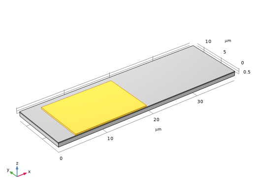
Locate the Selections of Resulting Entities section. Find the Cumulative selection subsection. From the Contribute to list, choose Polysilicon Beam.
|
|
5
|
|
1
|
|
2
|
|
3
|
|
4
|
|
5
|
|
1
|
|
2
|
|
3
|
Click in the Graphics window and then press Ctrl+A to select all objects.
|
|
4
|
|
5
|
|
6
|
|
7
|
|
8
|
Click
|
|
9
|
|
10
|
Click
|
|
1
|
|
2
|
Go to the Add Material window.
|
|
3
|
|
4
|
Click the Add to Component button in the window toolbar.
|
|
5
|
|
6
|
Click the Add to Component button in the window toolbar.
|
|
7
|
|
8
|
Click the Add to Component button in the window toolbar.
|
|
9
|
|
1
|
|
2
|
|
1
|
|
2
|
|
3
|
|
1
|
|
1
|
|
1
|
|
2
|
|
3
|
|
4
|
Click
|
|
1
|
|
2
|
|
3
|
|
4
|
|
1
|
|
2
|
In the Model Builder window, expand the Results > Mode Shape (solid) > Surface 1 node, then click Surface 1.
|
|
3
|
|
4
|
Click
|