PDF

Aluminum Nitride Lamb Wave Resonator — 3D
Introduction
This tutorial demonstrates how to model an aluminum nitride Lamb wave resonator in 3D. The Lamb wave resonator (LWR) is an important building block in circuits used in mobile communication systems. Its operational characteristics are controlled by the piezoelectric material properties, the pattern of thin conducting layer on its surface, and its dimensions. Using the Piezoeletricity multiphysics interface and material models from the Piezoelectric Material Library, you can create a digital prototype of an LWR.
Model Definition
In this tutorial, the LWR is an aluminum nitride (piezoelectric ) block with an interdigitated electrode (IDE) on its surface as shown in Figure 1. Suspended from four anchor points, the 0.4 μm piezoelectric block responds to AC excitation through the platinum IDE (80 nm). The LWR is designed to resonate at 8 GHz. The thin platinum layer was specified using the Thin Film feature in the Solid Mechanics Interface.
The LWR geometric parameters are summarized in the first table in the Modeling Instructions section so the geometry can be easily modified for design optimization. The geometry is rebuilt automatically when geometric parameters are changed if the rules are followed. For example, n must be chosen so (n+1)/4 is an integer, or = {3, 7, 11, …}. Also, the overlap parameter op should be smaller than the length of the finger l, that is, op < l. Keep in mind, however, that changes in the geometry will shift the resonant frequency. An outline of the steps in the fabrication of an actual LWR can be found in Ref. 1.
In this model, the fully coupled structural and electrostatic equations are solved in the piezoelectric domain. The model also includes mechanical loss through an isotropic structural loss factor of 0.002 for the piezoelectric and the platinum layers.
In this tutorial we are interested in the symmetric S0 mode, which, in typical applications, results in maximal electromechanical coupling efficiency. Because of the symmetry of the device structure and the symmetry of the S0 mode, only a half of the device needs to be modeled. This reduces computational time, which is important because this model requires a fine mesh (Figure 2) to compute accurate eigenmodes.
This tutorial shows you the setup of Eigenfrequency and Frequency Domain studies. In the Eigenfrequency study you investigate the eigenmodes of the structure to find the S0 mode. In the subsequent Frequency Domain study, a 1 V drive signal is applied to the Signal electrode and the resonator’s frequency response from 7.95 to 8.05 GHz is analyzed.
Figure 1: The geometric model of one half of the Lamb wave resonator. The interdigitated electrodes (IDE) are patterned from a thin layer of platinum (80 nm) on the top surface of the piezoelectric aluminum nitride block (0.4 μm).
Figure 2: The top surface of the LWR is meshed using Free Quad with maximum mesh size of 0.1 μm for accuracy and smooth surface plots.
Results and Discussion
Figure 3 shows the displacement in the z direction for the S0 mode at 7.993 GHz. In high-frequency resonant devices such as LWRs, the Eigenfrequency study returns many extraneous solutions very close to the mode of interest. Only through visual inspection can you identify the correct mode from among the spurious modes. Figure 4 shows the solid displacement across the XZ cut plane through the center of the resonator to verify the S0 mode.
Figure 3: 3D plot showing the pattern of the displacement along the z-axis for the S0 mode at 7.99 GHz.
Figure 4: Slice plot of solid displacement across the XZ cut plane through the center of the resonator for the S0 mode at 7.99 GHz.
Figure 5 is a log plot of the admittance magnitude versus frequency from 7.95 to 8.05 GHz. The plot is annotated with the positions of resonance and anti-resonance peaks for the calculation of the electromechanical coupling coefficient.
Figure 5: Admittance versus frequency.
The frequency response yields important information relating to device performance such as the effective electromechanical coupling coefficient given by
where fs and fp are the resonance and anti-resonance frequencies, respectively. With fs = 7.99 and fp = 8.04, kt2 = 1.5%. The effective electromechanical coupling coefficient is known to be a measure of transduction efficiency for conversion of electrical into mechanical energy.
Reference
1. J. Zou, C.M. Lin, A. Gao, and A.P. Pisano, “The Multi-Mode Resonance in AlN Lamb Wave Resonators,” J. Microelectromech. Syst., vol. 27, no. 6, pp. 973–84, 2018.
Application Library path: MEMS_Module/Piezoelectric_Devices/aln_lamb_wave_resonator_3d
Modeling Instructions
From the File menu, choose New.
New
In the New window, click  Model Wizard.
Model Wizard
1
In the Model Wizard window, click  3D.
Start by creating a new 3D model with a Piezoelectricity multiphysics interface.
2
In the Select Physics tree, select AC/DC > Electromagnetics and Mechanics > Piezoelectricity > Piezoelectricity, Solid.
3
Click Add.
4
Click  Study.
5
In the Select Study tree, select Preset Studies for Selected Multiphysics > Eigenfrequency.
6
Geometry 1
Use microns as the geometry unit.
1
In the Model Builder window, under Component 1 (comp1) click Geometry 1.
2
In the Settings window for Geometry, locate the Units section.
3
From the Length unit list, choose µm.
Define and specify the parameters of the model.
Global Definitions
Parameters 1
1
In the Model Builder window, under Global Definitions click Parameters 1.
2
In the Settings window for Parameters, locate the Parameters section.
3
Create the geometry model for half of the lamb wave resonator.
Geometry 1
Work Plane 1 (wp1)
1
In the Model Builder window, expand the Component 1 (comp1) > Geometry 1 node.
2
Right-click Geometry 1 and choose Work Plane.
Work Plane 1 (wp1) > Rectangle 1 (r1)
1
In the Work Plane toolbar, click  Rectangle.
2
In the Settings window for Rectangle, locate the Size and Shape section.
3
In the Width text field, type wf.
4
In the Height text field, type l.
5
Locate the Position section. From the Base list, choose Center.
6
In the yw text field, type dy/2.
Work Plane 1 (wp1) > Array 1 (arr1)
1
In the Work Plane toolbar, click  Transforms and choose Array.
2
3
In the Settings window for Array, locate the Size section.
4
In the xw size text field, type (n+1)/4.
5
Locate the Displacement section. In the xw text field, type 4*wf.
Work Plane 1 (wp1) > Move 1 (mov1)
1
In the Work Plane toolbar, click  Transforms and choose Move.
2
Click the  Select All button in the Graphics toolbar.
3
In the Settings window for Move, locate the Input section.
4
Select the Keep input objects checkbox.
5
Locate the Displacement section. In the xw text field, type 2*wf.
6
In the yw text field, type -dy.
Work Plane 1 (wp1) > Rectangle 2 (r2)
1
In the Work Plane toolbar, click  Rectangle.
2
In the Settings window for Rectangle, locate the Size and Shape section.
3
In the Width text field, type (n-1/2)*wf+we.
4
In the Height text field, type 2*wf.
5
Locate the Position section. In the yw text field, type (l+dy)/2.
Work Plane 1 (wp1) > Rectangle 3 (r3)
1
In the Work Plane toolbar, click  Rectangle.
2
In the Settings window for Rectangle, locate the Size and Shape section.
3
In the Width text field, type 2*we.
4
In the Height text field, type la.
5
Locate the Position section. In the xw text field, type (n-1/2)*wf-we.
6
In the yw text field, type (l+dy)/2+2*wf.
Work Plane 1 (wp1) > Mirror 1 (mir1)
1
In the Work Plane toolbar, click  Transforms and choose Mirror.
2
Select the objects r2 and r3 only.
3
In the Settings window for Mirror, locate the Input section.
4
Select the Keep input objects checkbox.
5
Locate the Normal Vector to Line of Reflection section. In the xw text field, type 0.
6
In the yw text field, type -1.
Work Plane 1 (wp1) > Rectangle 4 (r4)
1
In the Work Plane toolbar, click  Rectangle.
2
In the Settings window for Rectangle, locate the Size and Shape section.
3
In the Width text field, type (n+1/2)*wf.
4
In the Height text field, type l+dy.
5
Locate the Position section. From the Base list, choose Center.
6
In the xw text field, type (n+1/2)*wf/2.
Work Plane 1 (wp1) > Partition Objects 1 (par1)
1
In the Work Plane toolbar, click  Booleans and Partitions and choose Partition Objects.
2
Select the object arr1(1,1) only.
3
In the Settings window for Partition Objects, locate the Partition Objects section.
4
Click to select the  Activate Selection toggle button for Tool objects.
5
6
Select the Keep tool objects checkbox.
Work Plane 1 (wp1) > Delete Entities 1 (del1)
1
In the Model Builder window, right-click Plane Geometry and choose Delete Entities.
2
In the Settings window for Delete Entities, locate the Entities or Objects to Delete section.
3
From the Geometric entity level list, choose Domain.
4
On the object par1, select Domain 1 only.
Extrude 1 (ext1)
1
In the Model Builder window, right-click Geometry 1 and choose Extrude.
2
In the Settings window for Extrude, locate the Distances section.
3
4
Click  Build Selected.
5
Click the  Zoom Extents button in the Graphics toolbar.
Define selections for the electrodes and other boundaries. This will make specifying the material models and physics interface settings easier.
Definitions
Signal
1
In the Model Builder window, expand the Component 1 (comp1) > Definitions node.
2
Right-click Definitions and choose Selections > Box.
3
In the Settings window for Box, type Signal in the Label text field.
4
Locate the Geometric Entity Level section. From the Level list, choose Boundary.
5
Locate the Box Limits section. In the y minimum text field, type -l/2.
6
In the z minimum text field, type tp-0.01.
7
Locate the Output Entities section. From the Include entity if list, choose Entity inside box.
Ground
1
Right-click Signal and choose Duplicate.
2
In the Settings window for Box, type Ground in the Label text field.
3
Locate the Box Limits section. In the y minimum text field, type -Inf.
4
In the y maximum text field, type l/2.
Electrodes
1
In the Definitions toolbar, click  Union.
2
In the Settings window for Union, type Electrodes in the Label text field.
3
Locate the Geometric Entity Level section. From the Level list, choose Boundary.
4
Locate the Input Entities section. Under Selections to add, click  Add.
5
In the Add dialog, in the Selections to add list, choose Signal and Ground.
6
Symmetry
1
In the Definitions toolbar, click  Box.
2
In the Settings window for Box, type Symmetry in the Label text field.
3
Locate the Geometric Entity Level section. From the Level list, choose Boundary.
4
Locate the Box Limits section. In the x maximum text field, type 0.
5
Locate the Output Entities section. From the Include entity if list, choose Entity inside box.
Top Surface
1
In the Definitions toolbar, click  Box.
2
In the Settings window for Box, type Top Surface in the Label text field.
3
Locate the Geometric Entity Level section. From the Level list, choose Boundary.
4
Locate the Box Limits section. In the z minimum text field, type tp-0.01.
5
Locate the Output Entities section. From the Include entity if list, choose Entity inside box.
Device
1
In the Definitions toolbar, click  Box.
2
In the Settings window for Box, type Device in the Label text field.
3
Locate the Geometric Entity Level section. From the Level list, choose Boundary.
4
Locate the Box Limits section. In the y minimum text field, type -((l+dy)/2+2*wf+la)+0.01.
5
In the y maximum text field, type (l+dy)/2+2*wf+la-0.01.
Fixed Constraints
1
In the Definitions toolbar, click  Complement.
2
In the Settings window for Complement, type Fixed Constraints in the Label text field.
3
Locate the Geometric Entity Level section. From the Level list, choose Boundary.
4
Locate the Input Entities section. Under Selections to invert, click  Add.
5
In the Add dialog, select Device in the Selections to invert list.
6
Specify the settings for the Electrostatics interface.
Electrostatics (es)
Boundary Terminal 1
1
In the Physics toolbar, click  Boundaries and choose Boundary Terminal.
2
In the Settings window for Boundary Terminal, locate the Boundary Selection section.
3
From the Selection list, choose Signal.
4
Locate the Terminal section. From the Terminal type list, choose Voltage.
5
In the V0 text field, type Vapp.
Ground 1
1
In the Physics toolbar, click  Boundaries and choose Ground.
2
In the Settings window for Ground, locate the Boundary Selection section.
3
From the Selection list, choose Ground.
Symmetry Plane 1
1
In the Physics toolbar, click  Boundaries and choose Symmetry Plane.
2
In the Settings window for Symmetry Plane, locate the Boundary Selection section.
3
From the Selection list, choose Symmetry.
Specify the settings for the Solid Mechanics interface.
Solid Mechanics (solid)
Piezoelectric Material 1
In the Model Builder window, under Component 1 (comp1) > Solid Mechanics (solid) click Piezoelectric Material 1.
Mechanical Damping 1
1
In the Physics toolbar, click  Attributes and choose Mechanical Damping.
2
In the Settings window for Mechanical Damping, locate the Damping Settings section.
3
From the Damping type list, choose Isotropic loss factor.
Thin Layer 1
1
In the Physics toolbar, click  Boundaries and choose Thin Layer.
2
In the Settings window for Thin Layer, locate the Boundary Selection section.
3
From the Selection list, choose Electrodes.
4
Locate the Boundary Properties section. In the Lth text field, type 80[nm].
Linear Elastic Material 1
In the Model Builder window, expand the Component 1 (comp1) > Solid Mechanics (solid) > Thin Layer 1 > Linear Elastic Material 1 node, then click Linear Elastic Material 1.
Damping 1
1
In the Physics toolbar, click  Attributes and choose Damping.
2
In the Settings window for Damping, locate the Damping Settings section.
3
From the Damping type list, choose Isotropic loss factor.
Fixed Constraint 1
1
In the Physics toolbar, click  Boundaries and choose Fixed Constraint.
2
In the Settings window for Fixed Constraint, locate the Boundary Selection section.
3
From the Selection list, choose Fixed Constraints.
Symmetry 1
1
In the Physics toolbar, click  Boundaries and choose Symmetry.
2
In the Settings window for Symmetry, locate the Boundary Selection section.
3
From the Selection list, choose Symmetry.
Add materials to the model and specify the regions they belong to.
Add Material
1
In the Home toolbar, click  Add Material to open the Add Material window.
2
Go to the Add Material window.
3
In the tree, select MEMS > Metals > Pt - Platinum.
4
Click the Add to Component button in the window toolbar.
Materials
Pt - Platinum (mat1)
1
In the Settings window for Material, locate the Geometric Entity Selection section.
2
From the Geometric entity level list, choose Boundary.
3
From the Selection list, choose Electrodes.
4
Locate the Material Contents section. In the table, enter the following settings:
Add Material
1
Go to the Add Material window.
2
In the tree, select Piezoelectric > Aluminum Nitride.
3
Click the Add to Component button in the window toolbar.
4
In the Materials toolbar, click  Add Material to close the Add Material window.
Materials
Aluminum Nitride (mat2)
1
In the Settings window for Material, locate the Geometric Entity Selection section.
2
From the Selection list, choose All domains.
3
Locate the Material Contents section. In the table, enter the following settings:
Create the mesh for the model.
Mesh 1
Free Quad 1
1
In the Mesh toolbar, click  More Generators and choose Free Quad.
2
In the Settings window for Free Quad, locate the Boundary Selection section.
3
From the Selection list, choose Top Surface.
Size 1
1
Right-click Free Quad 1 and choose Size.
2
In the Settings window for Size, locate the Element Size section.
3
Click the Custom button.
4
Locate the Element Size Parameters section.
5
Select the Maximum element size checkbox. In the associated text field, type 0.1.
6
Click  Build Selected.
Swept 1
In the Mesh toolbar, click  Swept.
Distribution 1
1
Right-click Swept 1 and choose Distribution.
2
In the Settings window for Distribution, locate the Distribution section.
3
In the Number of elements text field, type 3.
4
Click  Build Selected.
Set up an Eigenfrequency study to search for an eigenfrequency around 8 GHz.
Eigenfrequency
1
In the Model Builder window, click Study 1.
2
In the Settings window for Study, type Eigenfrequency in the Label text field.
3
Locate the Study Settings section. Clear the Generate default plots checkbox.
Step 1: Eigenfrequency
1
In the Model Builder window, under Eigenfrequency click Step 1: Eigenfrequency.
2
In the Settings window for Eigenfrequency, locate the Study Settings section.
3
Select the Desired number of eigenfrequencies checkbox. In the associated text field, type 20.
4
From the Unit list, choose GHz.
5
In the Search for eigenfrequencies around shift text field, type 8.
6
In the Study toolbar, click  Compute.
Add a Mirror dataset to complete the device structure. This dataset will be used to plot the result of the Eigenfrequency study.
Results
Mirror 3D 1
1
In the Model Builder window, expand the Results node.
2
Right-click Results > Datasets and choose More 3D Datasets > Mirror 3D.
3
In the Settings window for Mirror 3D, click  Plot.
With the solution from the Eigenfrequency study, create a 3D plot to display the shape of the eigenmode at 8 GHz. Use the Mirror dataset previously created.
Mode Shape
1
In the Results toolbar, click  3D Plot Group.
2
In the Settings window for 3D Plot Group, type Mode Shape in the Label text field.
3
Locate the Data section. From the Dataset list, choose Mirror 3D 1.
4
From the Eigenfrequency (GHz) list, choose 7.993+0.0079481i.
5
Locate the Plot Settings section. Clear the Plot dataset edges checkbox.
Surface 1
1
Right-click Mode Shape and choose Surface.
2
In the Settings window for Surface, locate the Expression section.
3
In the Expression text field, type w.
4
Select the Description checkbox.
5
In the Mode Shape toolbar, click  Plot.
6
Click the  Go to XY View button in the Graphics toolbar.
7
Click the  Go to XY View button in the Graphics toolbar.
8
Click the  Go to XY View button in the Graphics toolbar.
With the solution from the Eigenfrequency study, create a Slice plot to display the eigenmode in the xz cut plane through the center.
Mode Shape
In the Model Builder window, click Mode Shape.
Mode Shape, Center XZ Plane
1
In the Results toolbar, click  3D Plot Group.
2
In the Settings window for 3D Plot Group, type Mode Shape, Center XZ Plane in the Label text field.
3
Locate the Data section. From the Dataset list, choose Mirror 3D 1.
4
From the Eigenfrequency (GHz) list, choose 7.993+0.0079481i.
Slice 1
1
Right-click Mode Shape, Center XZ Plane and choose Slice.
2
In the Settings window for Slice, locate the Expression section.
3
In the Expression text field, type solid.disp.
4
Select the Description checkbox.
5
Locate the Plane Data section. From the Plane list, choose zx-planes.
6
In the Planes text field, type 1.
7
Locate the Coloring and Style section. From the Color table type list, choose Discrete.
8
In the Number of bands text field, type 15.
Mode Shape, Center XZ Plane
1
In the Model Builder window, click Mode Shape, Center XZ Plane.
2
In the Settings window for 3D Plot Group, locate the Plot Settings section.
3
Clear the Plot dataset edges checkbox.
4
In the Mode Shape, Center XZ Plane toolbar, click  Plot.
5
Click the  Go to XZ View button in the Graphics toolbar.
Set up a Frequency Domain study with a range that includes the features of interest, for example, resonance and anti-resonance peaks. Disable the option to generate default plots from this study.
Add Study
1
In the Home toolbar, click  Add Study to open the Add Study window.
2
Go to the Add Study window.
3
Find the Studies subsection. In the Select Study tree, select General Studies > Frequency Domain.
4
Click the Add Study button in the window toolbar.
5
In the Home toolbar, click  Add Study to close the Add Study window.
Frequency Domain - 7.95 to 8.05 GHz
1
In the Settings window for Study, type Frequency Domain - 7.95 to 8.05 GHz in the Label text field.
2
Locate the Study Settings section. Clear the Generate default plots checkbox.
Step 1: Frequency Domain
1
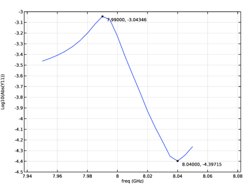
In the Model Builder window, under Frequency Domain - 7.95 to 8.05 GHz click Step 1: Frequency Domain.
2
In the Settings window for Frequency Domain, locate the Study Settings section.
3
From the Frequency unit list, choose GHz.
4
Click  Range.
5
In the Range dialog, type 7.95 in the Start text field.
6
In the Step text field, type 0.005.
7
In the Stop text field, type 8.05.
8
Click Add.
9
In the Study toolbar, click  Compute.
With the solution from Frequency Domain study, plot the admittance versus frequency and add a Graph Marker to return the coordinates of the maximum and minimum values.
Results
Frequency Domain
1
In the Results toolbar, click  1D Plot Group.
2
In the Settings window for 1D Plot Group, type Frequency Domain in the Label text field.
3
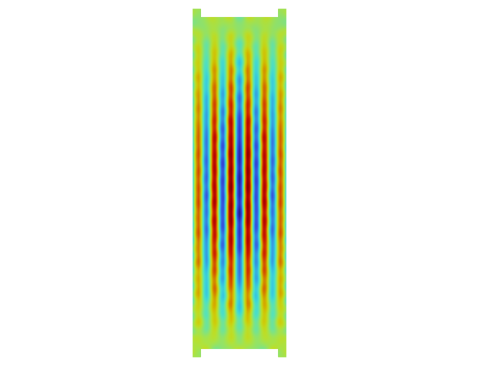
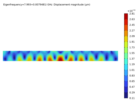
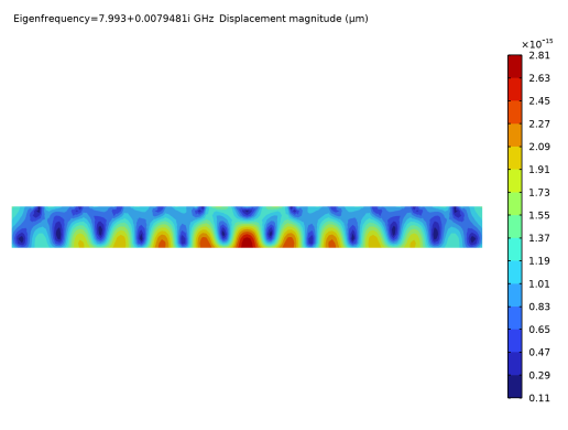
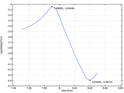
Locate the Data section. From the Dataset list, choose Frequency Domain - 7.95 to 8.05 GHz/Solution 2 (sol2).
4
Locate the Plot Settings section.
5
Select the y-axis label checkbox. In the associated text field, type Log10(Abs(Y11)).
Global 1
1
Right-click Frequency Domain and choose Global.
2
In the Settings window for Global, locate the y-Axis Data section.
3
4
Click to expand the Legends section. Find the Include subsection. Clear the Description checkbox.
Graph Marker 1
1
Right-click Global 1 and choose Graph Marker.
2
In the Settings window for Graph Marker, locate the Text Format section.
3
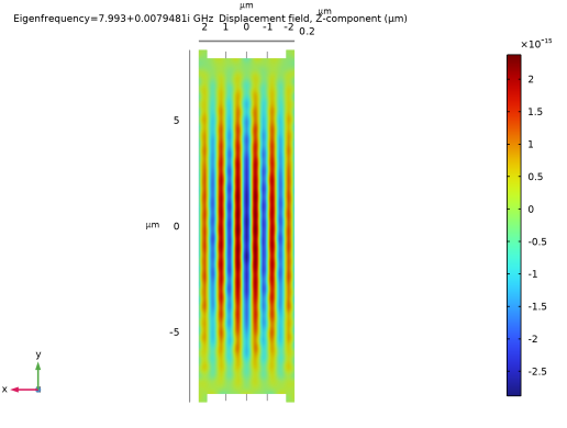
Select the Show x-coordinate checkbox.
4
In the Frequency Domain toolbar, click  Plot.