PDF

Partial Discharge Inside Solid Dielectrics
Introduction
The electrical insulation strength of gases is generally much lower than that of solid dielectrics. As a result, small voids, cracks, or imperfections within solid insulation can give rise to localized electrical discharges, commonly referred to as partial discharges (PDs). Although these discharges do not bridge the entire insulation system, they can gradually degrade the material, leading to long-term insulation failure. For this reason, partial discharge detection and analysis are widely used in high-voltage engineering as a diagnostic tool for assessing insulation condition.
This model simulates partial discharges in a spherical air void embedded within a solid dielectric subjected to a 50 Hz AC power frequency. The formulation includes detailed charge transport processes for electrons and ions, fully coupled with electrostatics. Surface charge accumulation at the gas–solid interface is also treated self-consistently, as it plays a key role in the development and quenching of the discharge.
The simulation outputs the Phase-Resolved Partial Discharge (PRPD) pattern, which provides insight into the timing, magnitude, and polarity of discharges relative to the applied voltage cycle. These results can be compared directly with experimental measurements, offering a valuable tool for studying the mechanisms of partial discharge initiation and progression in solid insulation systems.
Model Definition
The Electric Discharge interface is used to simulate the partial discharge. The built-in charge transport model is used:
where
e, p, n denote electrons, positive ions, and negative ions
ni is the number density of the charge carrier (SI unit: 1/m3)
E is the electric field (SI unit: V/m)
zi denotes the carrier charge (SI unit: 1)
μi denotes the carrier mobility (SI unit: m2/(V·s))
wi is the drift velocity in the electric field (SI unit: m/s)
Di is the diffusion coefficient (SI unit: m2/s)
Ri is the reaction rate (SI unit: 1/(m3·s))
α is the ionization coefficient (SI unit: 1/m)
η is the attachment coefficient (SI unit: 1/m)
βep is the electron–ion recombination coefficient (SI unit: m3/s)
βpn is the ion–ion recombination coefficient (SI unit: m3/s)
The above transport equations are fully coupled with Poisson’s equation through the electric field and the space charge:
where e is the elementary charge.
The Gas–Solid interface is modeled with the dedicated Dielectric Interface, Surface Transport feature described in the Electric Discharge Module User’s Guide.
Results and Discussion
Figure 1 shows the PRPD measured by discharge current as a function of phase angle. Figure 2 shows the surface charge density at the void-solid interface as a function of direction angle for several time instants.
Figure 1: The partial discharge current as a function phase angle.
Figure 2: The distribution of surface charge density at the void-solid interface.
Figure 3: The distribution of electric field at different phase angles.
Application Library path: Electric_Discharge_Module/Partial_Discharges/partial_discharge
Modeling Instructions
From the File menu, choose New.
New
In the New window, click  Model Wizard.
Model Wizard
1
In the Model Wizard window, click  2D Axisymmetric.
2
In the Select Physics tree, select Electric Discharge > Electric Discharge (edis).
3
Click Add.
4
Click  Study.
5
In the Select Study tree, select Preset Studies for Selected Physics Interfaces > Time Dependent with Initialization.
6
Geometry 1
1
In the Model Builder window, under Component 1 (comp1) click Geometry 1.
2
In the Settings window for Geometry, locate the Units section.
3
From the Length unit list, choose mm.
Rectangle 1 (r1)
1
In the Geometry toolbar, click  Rectangle.
2
In the Settings window for Rectangle, locate the Size and Shape section.
3
In the Width text field, type 2.
4
In the Height text field, type 2.
5
Locate the Position section. In the z text field, type -1.
Circle 1 (c1)
1
In the Geometry toolbar, click  Circle.
2
In the Settings window for Circle, locate the Size and Shape section.
3
In the Radius text field, type 0.5.
4
In the Sector angle text field, type 180.
5
Locate the Rotation Angle section. In the Rotation text field, type -90.
6
Click  Build All Objects.
Global Definitions
Parameters 1
1
In the Model Builder window, under Global Definitions click Parameters 1.
2
In the Settings window for Parameters, locate the Parameters section.
3
Add Material from Library
In the Home toolbar, click  Windows and choose Add Material from Library.
Add Material
1
Go to the Add Material window.
2
In the tree, select Electric Discharge > Gases > Air > Air [Kang et al. 2003].
3
Right-click and choose Add to Component 1 (comp1).
Materials
Air [Kang et al. 2003] (mat1)
1
In the Model Builder window, under Component 1 (comp1) > Materials click Air [Kang et al. 2003] (mat1).
2
Electric Discharge (edis)
1
In the Model Builder window, under Component 1 (comp1) click Electric Discharge (edis).
2
In the Settings window for Electric Discharge, locate the Physical Model section.
3
Select the Solid checkbox.
Enable the isotropic diffusion stabilization.
4
Click the  Show More Options button in the Model Builder toolbar.
5
In the Show More Options dialog, select Physics > Stabilization in the tree.
6
7
8
In the Settings window for Electric Discharge, click to expand the Inconsistent Stabilization section.
9
Select the Isotropic diffusion checkbox.
Gas 1
1
In the Model Builder window, under Component 1 (comp1) > Electric Discharge (edis) click Gas 1.
2
Solid 1
1
In the Model Builder window, click Solid 1.
2
3
In the Settings window for Solid, locate the Model Formulation section.
4
From the Material model list, choose Insulator.
5
Locate the Constitutive Relation D-E section. From the εr list, choose User defined. In the associated text field, type 4.3.
Electrode 1
1
In the Physics toolbar, click  Attributes and choose Electrode.
2
3
In the Settings window for Electrode, locate the Terminal section.
4
In the V0 text field, type Va.
Solid 1
In the Model Builder window, click Solid 1.
Electrode 2
1
In the Physics toolbar, click  Attributes and choose Electrode.
2
Mesh 1
1
In the Model Builder window, under Component 1 (comp1) click Mesh 1.
2
In the Settings window for Mesh, locate the Sequence Type section.
3
From the list, choose User-controlled mesh.
Size 1
1
In the Model Builder window, right-click Free Triangular 1 and choose Size.
2
In the Settings window for Size, locate the Geometric Entity Selection section.
3
From the Geometric entity level list, choose Domain.
4
5
Locate the Element Size section. Click the Custom button.
6
Locate the Element Size Parameters section.
7
Select the Maximum element size checkbox. In the associated text field, type 20[um].
Boundary Layers 1
1
In the Mesh toolbar, click  Boundary Layers.
2
In the Settings window for Boundary Layers, locate the Domain Selection section.
3
From the Geometric entity level list, choose Domain.
4
Boundary Layer Properties
1
In the Model Builder window, click Boundary Layer Properties.
2
3
In the Settings window for Boundary Layer Properties, click  Build All.
Study 1
Step 2: Time Dependent
1
In the Model Builder window, expand the Component 1 (comp1) > Definitions node, then click Study 1 > Step 2: Time Dependent.
2
In the Settings window for Time Dependent, locate the Study Settings section.
3
In the Output times text field, type range(0,1/f/20,2/f).
Definitions
Global Variable Probe 1 (var1)
1
In the Definitions toolbar, click  Probes and choose Global Variable Probe.
2
In the Settings window for Global Variable Probe, type I0 in the Variable name text field.
3
Locate the Expression section. In the Expression text field, type edis.I0_0.
4
In the Table and plot unit field, type uA.
Global Variable Probe 2 (var2)
1
In the Definitions toolbar, click  Probes and choose Global Variable Probe.
2
In the Settings window for Global Variable Probe, type phase in the Variable name text field.
3
Locate the Expression section. In the Expression text field, type mod(2*pi*f*t,2*pi).
4
In the Table and plot unit field, type deg.
5
Select the Description checkbox. In the associated text field, type Phase angle.
Study 1
1
In the Model Builder window, click Study 1.
2
In the Settings window for Study, locate the Study Settings section.
3
Clear the Generate default plots checkbox.
4
In the Study toolbar, click  Compute.
Results
Probe Table Graph 1
1
In the Model Builder window, expand the Probe Plot Group 1 node, then click Probe Table Graph 1.
2
In the Settings window for Table Graph, locate the Data section.
3
In the Columns list box, select Terminal current (uA).
4
From the x-axis data list, choose Phase angle (deg).
5
Locate the Coloring and Style section. Find the Line style subsection. From the Line list, choose None.
6
Find the Line markers subsection. From the Marker list, choose Circle.
7
From the Positioning list, choose In data points.
Global 1
1
In the Model Builder window, right-click Probe Plot Group 1 and choose Global.
2
In the Settings window for Global, locate the y-Axis Data section.
3
4
Locate the x-Axis Data section. From the Parameter list, choose Expression.
5
In the Expression text field, type 2*pi*f*t.
6
In the Unit field, type deg.
7
Locate the Data section. From the Dataset list, choose Study 1/Solution 1 (sol1).
8
From the Time selection list, choose From list.
9
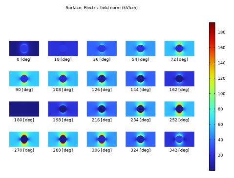
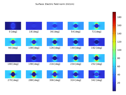
In the Times (s) list, choose 0, 0.001, 0.002, 0.003, 0.004, 0.005, 0.006, 0.007, 0.008, 0.009, 0.01, 0.011, 0.012, 0.013, 0.014, 0.015, 0.016, 0.017, 0.018, 0.019, and 0.02.
Probe Plot Group 1
1
In the Model Builder window, click Probe Plot Group 1.
2
In the Settings window for 1D Plot Group, locate the Plot Settings section.
3
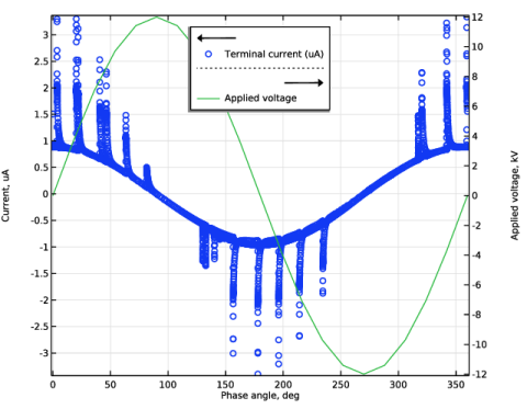
Select the Two y-axes checkbox.
4
Select the x-axis label checkbox. In the associated text field, type Phase angle, deg.
5
Select the y-axis label checkbox. In the associated text field, type Current, uA.
6
Select the Secondary y-axis label checkbox. In the associated text field, type Applied voltage, kV.
7
In the table, select the Plot on secondary y-axis checkbox for Global 1.
8
Locate the Legend section. From the Position list, choose Upper middle.
9
Click to expand the Title section. From the Title type list, choose None.
10
In the Probe Plot Group 1 toolbar, click  Plot.
Surface Charge Density
1
In the Results toolbar, click  1D Plot Group.
2
In the Settings window for 1D Plot Group, type Surface Charge Density in the Label text field.
Line Graph 1
1
Right-click Surface Charge Density and choose Line Graph.
2
3
In the Settings window for Line Graph, locate the y-Axis Data section.
4
In the Expression text field, type edis.rhos.
5
In the Unit field, type nC/mm^2.
6
Locate the x-Axis Data section. From the Parameter list, choose Expression.
7
In the Expression text field, type atan(z/r).
8
In the Unit field, type deg.
9
Select the Description checkbox. In the associated text field, type Direction angle.
10
Click to expand the Coloring and Style section. Find the Line markers subsection. From the Marker list, choose Cycle.
11
From the Positioning list, choose Interpolated.
12
Click to expand the Legends section. Select the Show legends checkbox.
Surface Charge Density
1
In the Model Builder window, click Surface Charge Density.
2
In the Settings window for 1D Plot Group, locate the Data section.
3
From the Time selection list, choose Interpolated.
4
In the Times (s) text field, type range(1/f,1/f/5,2/f).
5
Locate the Title section. From the Title type list, choose None.
6
Locate the Legend section. From the Position list, choose Upper middle.
7
In the Surface Charge Density toolbar, click  Plot.
Mirror 2D 1
1
In the Model Builder window, expand the Results > Datasets node.
2
Right-click Results > Datasets and choose More 2D Datasets > Mirror 2D.
2D Plot Group 3
In the Results toolbar, click  2D Plot Group.
Surface 1
1
In the Model Builder window, right-click 2D Plot Group 3 and choose Surface.
2
In the Settings window for Surface, locate the Expression section.
3
In the Expression text field, type edis.normE.
4
In the Unit field, type kV/cm.
Solution Array 1
Right-click Surface 1 and choose Solution Array.
2D Plot Group 3
1
In the Settings window for 2D Plot Group, locate the Data section.
2
From the Dataset list, choose Mirror 2D 1.
3
Locate the Plot Settings section. Clear the Plot dataset edges checkbox.
4
In the 2D Plot Group 3 toolbar, click  Plot.
Solution Array 1
1
In the Model Builder window, under Results > 2D Plot Group 3 > Surface 1 click Solution Array 1.
2
In the Settings window for Solution Array, locate the Data section.
3
From the Time selection list, choose From list.
4
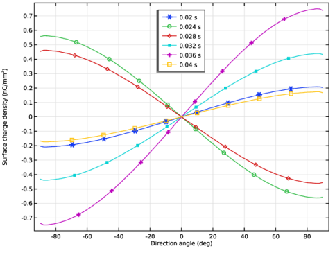
In the Times (s) list, choose 0.02, 0.021, 0.022, 0.023, 0.024, 0.025, 0.026, 0.027, 0.028, 0.029, 0.03, 0.031, 0.032, 0.033, 0.034, 0.035, 0.036, 0.037, 0.038, and 0.039.
2D Plot Group 3
1
In the Model Builder window, under Results click 2D Plot Group 3.
2
In the Settings window for 2D Plot Group, click to expand the Plot Array section.
3
From the Array type list, choose Square.
4
In the Relative row padding text field, type -1.5.
Solution Array 1
1
In the Model Builder window, under Results > 2D Plot Group 3 > Surface 1 click Solution Array 1.
2
In the Settings window for Solution Array, locate the Plot Array section.
3
From the Array shape list, choose Square.
Annotation 1
In the Model Builder window, right-click 2D Plot Group 3 and choose Annotation.
Solution Array 1
In the Model Builder window, under Results > 2D Plot Group 3 > Surface 1 right-click Solution Array 1 and choose Copy.
Solution Array 1
In the Model Builder window, right-click Annotation 1 and choose Paste Solution Array.
Annotation 1
1
In the Settings window for Annotation, click to expand the Plot Array section.
2
Select the Manual indexing checkbox.
3
Locate the Position section. In the y text field, type -1.2.
4
Locate the Coloring and Style section. From the Anchor point list, choose Upper middle.
5
Clear the Show point checkbox.
6
Locate the Annotation section. In the Text text field, type eval(phase,deg,3) [deg].
7
Locate the Position section. In the y text field, type -1.
Electric Fields
1
In the Model Builder window, under Results click 2D Plot Group 3.
2
In the Settings window for 2D Plot Group, type Electric Fields in the Label text field.
3
Click to expand the Title section. From the Title type list, choose Custom.
4
Find the Solution subsection. Clear the Solution checkbox.
5
Click the  Show Grid button in the Graphics toolbar.
6
Click the  Zoom Extents button in the Graphics toolbar.
7
In the Electric Fields toolbar, click  Plot.