
|
|
|


|
1
|
|
2
|
In the Select Physics tree, select Electrochemistry > Primary and Secondary Current Distribution > Secondary Current Distribution (cd).
|
|
3
|
Click Add.
|
|
4
|
Click
|
|
5
|
|
6
|
Click
|
|
1
|
|
2
|
|
3
|
Click
|
|
4
|
Browse to the model’s Application Libraries folder and double-click the file pcb_designer_parameters.txt.
|
|
1
|
|
2
|
Browse to the model’s Application Libraries folder and double-click the file pcb_designer_geom_sequence.mph.
|
|
3
|
|
4
|
|
1
|
|
2
|
In the Settings window for Box Selection, type Electrolyte swept mesh region 2 in the Label text field.
|
|
3
|
|
4
|
|
1
|
|
2
|
In the Settings window for Union Selection, type Electrolyte swept mesh regions in the Label text field.
|
|
3
|
|
4
|
In the Add dialog, in the Selections to add list, choose Electrolyte swept mesh region 1 and Electrolyte swept mesh region 2.
|
|
5
|
Click OK.
|
|
6
|
|
1
|
|
2
|
|
3
|
|
4
|
|
5
|
Click OK.
|
|
6
|
|
7
|
|
8
|
Click
|
|
9
|
|
10
|
Click OK.
|
|
11
|
|
1
|
|
2
|
|
3
|
|
4
|
|
5
|
|
6
|
Click OK.
|
|
7
|
|
1
|
|
2
|
|
3
|
|
4
|
|
5
|
Click OK.
|
|
6
|
|
7
|
|
8
|
|
9
|
Click OK.
|
|
10
|
|
11
|
|
12
|
|
13
|
|
14
|
Click OK.
|
|
15
|
|
16
|
|
17
|
|
18
|
Click OK.
|
|
19
|
|
20
|
|
21
|
Clear the Automatic detection of small details checkbox.
|
|
22
|
|
1
|
|
2
|
|
3
|
|
4
|
|
1
|
|
2
|
|
3
|
Click
|
|
4
|
Browse to the model’s Application Libraries folder and double-click the file pcb_designer_variables.txt.
|
|
1
|
In the Model Builder window, under Component 1 (comp1) right-click Materials and choose Blank Material.
|
|
2
|
|
3
|
Locate the Material Contents section. In the table, enter the following settings:
|
|
1
|
|
2
|
|
3
|
|
4
|
Locate the Electrode Phase Potential Condition section. From the Electrode phase potential condition list, choose Total current.
|
|
5
|
|
1
|
|
2
|
|
3
|
|
4
|
|
5
|
|
1
|
|
2
|
|
3
|
|
1
|
|
2
|
|
3
|
|
4
|
|
5
|
|
1
|
In the Model Builder window, under Component 1 (comp1) > Secondary Current Distribution (cd) click Initial Values 1.
|
|
2
|
|
3
|
|
1
|
|
2
|
|
3
|
|
1
|
|
2
|
|
3
|
|
1
|
|
2
|
|
3
|
|
4
|
|
1
|
|
2
|
|
3
|
|
4
|
|
5
|
|
6
|
|
7
|
Click OK.
|
|
8
|
|
9
|
|
1
|
|
2
|
|
3
|
|
4
|
Click
|
|
5
|
|
6
|
Click OK.
|
|
7
|
|
8
|
|
1
|
|
2
|
|
3
|
In the Number of elements text field, type round((PCBThickness/1.5[mm]>=1)*PCBThickness/1.5[mm]+(PCBThickness/1.5[mm]<1),0).
|
|
1
|
|
2
|
|
3
|
|
4
|
Locate the Distribution section. In the Number of elements text field, type ((PCBOffset-PCBThickness)/2[mm]>=1)*(PCBOffset-PCBThickness)/2[mm]+((PCBOffset-PCBThickness)/2[mm]<1).
|
|
1
|
|
2
|
|
3
|
|
4
|
|
5
|
|
6
|
|
1
|
|
2
|
|
3
|
|
4
|
|
5
|
|
1
|
|
2
|
|
3
|
In the Number of elements text field, type (ApertureThickness/1.5[mm]>=1)*ApertureThickness/1.5[mm]+(ApertureThickness/1.5[mm]<1).
|
|
1
|
|
2
|
|
1
|
|
2
|
|
3
|
|
4
|
|
5
|
|
6
|
|
7
|
Clear the Generate default plots checkbox.
|
|
8
|
|
1
|
|
2
|
|
3
|
|
4
|
|
5
|
|
1
|
|
2
|
|
3
|
|
4
|
|
1
|
|
2
|
|
3
|
|
1
|
|
2
|
|
3
|
|
4
|
|
5
|
Click OK.
|
|
1
|
|
2
|
|
3
|
|
1
|
|
2
|
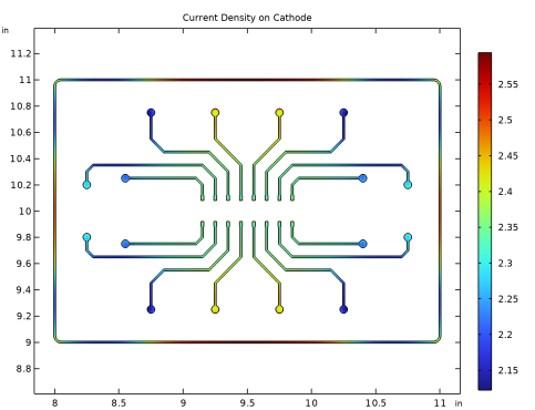
In the Settings window for Surface, click Replace Expression in the upper-right corner of the Expression section. From the menu, choose Component 1 (comp1) > Definitions > Variables > thickness_cathode - Thickness on cathode - m.
|
|
3
|
|
1
|
|
2
|
|
3
|
|
1
|
|
2
|
|
3
|
|
1
|
|
2
|
In the Settings window for Surface, click Replace Expression in the upper-right corner of the Expression section. From the menu, choose Component 1 (comp1) > Secondary Current Distribution > Electrode kinetics > cd.iloc_er1 - Local current density - A/m².
|
|
3
|
|
4
|
|
5
|
|
1
|
|
2
|
|
1
|
|
2
|
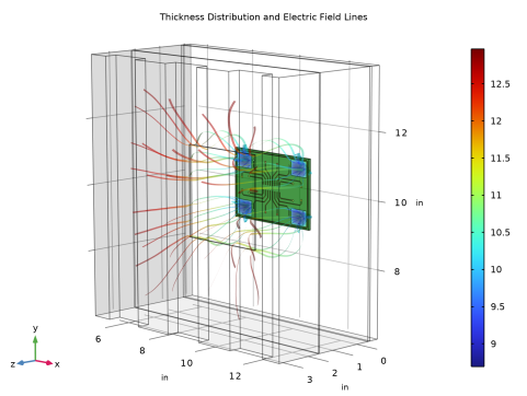
In the Settings window for 3D Plot Group, type Thickness Distribution and Electric Field Lines in the Label text field.
|
|
1
|
|
2
|
|
3
|
|
4
|
|
5
|
|
1
|
In the Model Builder window, right-click Thickness Distribution and Electric Field Lines and choose Surface.
|
|
2
|
|
3
|
|
4
|
|
5
|
|
6
|
|
7
|
Click Define custom colors.
|
|
9
|
Click Add to custom colors.
|
|
10
|
|
1
|
|
2
|
|
3
|
|
4
|
|
5
|
|
6
|
|
1
|
|
2
|
|
3
|
|
4
|
|
5
|
Locate the Coloring and Style section. Find the Line style subsection. From the Type list, choose Ribbon.
|
|
1
|
|
2
|
|
3
|
Clear the Color legend checkbox.
|
|
1
|
|
2
|
|
3
|
|
4
|
|
1
|
|
2
|
Click
|
|
1
|
|
2
|
|
3
|
Click
|
|
4
|
Browse to the model’s Application Libraries folder and double-click the file pcb_designer_geom_sequence_parameters.txt.
|
|
1
|
|
2
|
|
3
|
|
1
|
|
2
|
|
3
|
|
4
|
|
5
|
|
6
|
|
7
|
|
8
|
|
9
|
Locate the Selections of Resulting Entities section. Select the Resulting objects selection checkbox.
|
|
10
|
|
1
|
|
2
|
|
3
|
|
4
|
Locate the Selections of Resulting Entities section. Find the Cumulative selection subsection. Click New.
|
|
5
|
|
6
|
Click OK.
|
|
7
|
|
1
|
|
2
|
|
3
|
Click
|
|
4
|
|
5
|
Click
|
|
6
|
|
1
|
|
2
|
|
3
|
|
1
|
|
2
|
|
3
|
|
4
|
Locate the Selections of Resulting Entities section. Find the Cumulative selection subsection. Click New.
|
|
5
|
|
6
|
Click OK.
|
|
7
|
|
1
|
|
2
|
|
3
|
Click
|
|
4
|
Browse to the model’s Application Libraries folder and double-click the file example_pcb_dummy_pattern.tgz.
|
|
5
|
Click
|
|
6
|
|
1
|
|
2
|
|
1
|
|
2
|
|
3
|
|
4
|
|
5
|
|
6
|
Click OK.
|
|
1
|
|
2
|
|
3
|
|
4
|
|
5
|
|
6
|
|
7
|
|
8
|
Locate the Selections of Resulting Entities section. Select the Resulting objects selection checkbox.
|
|
1
|
|
2
|
|
3
|
|
4
|
|
5
|
|
6
|
|
7
|
|
8
|
|
9
|
Locate the Selections of Resulting Entities section. Select the Resulting objects selection checkbox.
|
|
1
|
|
2
|
|
3
|
|
4
|
|
5
|
On the object blk2, select Boundary 4 only.
|
|
6
|
Click
|
|
1
|
|
2
|
|
3
|
|
4
|
|
5
|
|
6
|
|
1
|
|
2
|
|
3
|
Select the object r1 only.
|
|
4
|
|
5
|
|
6
|
|
7
|
|
1
|
|
2
|
|
3
|
Locate the Distances section. In the table, enter the following settings:
|
|
4
|
Select the Reverse direction checkbox.
|
|
5
|
Locate the Selections of Resulting Entities section. Select the Resulting objects selection checkbox.
|
|
6
|
|
1
|
In the Model Builder window, right-click Geometry 1 and choose Booleans and Partitions > Difference.
|
|
2
|
|
3
|
|
4
|
|
5
|
|
6
|
|
1
|
|
2
|
|
3
|
|
1
|
|
2
|
|
3
|
|
4
|
Click
|
|
1
|
|
2
|
|
3
|
|
4
|
|
1
|
In the Model Builder window, collapse the Component 1 (comp1) > Geometry 1 > Work Plane 4 (wp4) node.
|
|
2
|
|
3
|
|
1
|
|
2
|
|
4
|
Click
|
|
1
|
|
2
|
Select the object dif1 only.
|
|
3
|
|
4
|
|
5
|
Select the object ext2 only.
|
|
6
|
Click
|
|
1
|
|
2
|
|
3
|
|
4
|
Locate the Selections of Resulting Entities section. Select the Resulting objects selection checkbox.
|
|
5
|
Click
|
|
1
|
|
2
|
|
3
|
|
4
|
|
5
|
Locate the Position section. In the xw text field, type PCBxMin-(BathWidth-PCBWidth)/2+(BathWidth-ApertureWidth)/2.
|
|
6
|
|
1
|
In the Model Builder window, collapse the Component 1 (comp1) > Geometry 1 > Aperture source (wp5) node.
|
|
2
|
|
3
|
|
1
|
|
2
|
|
3
|
Locate the Distances section. In the table, enter the following settings:
|
|
4
|
Locate the Selections of Resulting Entities section. Select the Resulting objects selection checkbox.
|