PDF

Aperture Shape Optimization for Electroplating of a Printed Circuit Board
Introduction
A printed circuit board (PCB) is the heart of almost any electronic product, carrying the components and copper wires supporting its functionality. This tutorial demonstrates how to simulate copper deposition on a PCB using the Secondary Current Distribution and Shape Optimization interfaces.
An aperture is typically used in the electroplating bath in order to achieve uniform deposition thickness across the PCB. The size and aspect ratio of the aperture are optimized using the Transformation feature in the Shape Optimization interface.
The PCB pattern in this example is defined by imported ECAD files.
Note: This model requires ECAD Import Module and Optimization Module licenses.
Model Definition
Figure 1 shows the model geometry.
Figure 1: Model geometry.
The anodes are a set of stretched blocks at the top of the geometry. The cathode is the PCB pattern located at the bottom-center of the electroplating bath. An isolating screen with an aperture is placed between the anodes and the cathode to control the current distribution on the PCB. Due to mirror symmetry, only one-fourth of the actual geometry is used in the model.
Charge Transport
The model uses the Secondary Current Distribution interface to simulate the current distribution in the electroplating bath. It solves for the electrolyte potential, ϕl (V), according to
where il (A/m2) is the electrolyte current density vector and σl (S/m) is the electrolyte conductivity, which is assumed to be a constant.
The default Insulation condition is used for all boundaries except the anode and cathode surfaces:
where n is the normal vector, pointing out of the domain.
The main electrode reaction on both the anode and the cathode surfaces is the copper deposition/dissolution reaction
A Butler–Volmer kinetics is used to model copper dissolution and deposition at the anode and cathode surfaces, respectively, which sets the local current density to
Note that the local current density is positive at the anode surface and negative at the cathode surfaces, depending on the sign of the overpotential, η (V), defined as
(1)
where Eeq (V) is the equilibrium potential of the copper dissolution/deposition reaction and ϕs (V) is the potential of the electronic phase of the electrode.
On both the anode and the cathode surfaces, the electrolyte current density is set to the local current density of the copper deposition reaction:
(2)
The anode is grounded in the model whereas the cathode electric potential is solved for by an additional equation in order to fulfill a total current condition on the boundary according to
(3)
The Thin Electrolyte Layer feature is used at the isolating screen. The Symmetry boundary condition is set at the appropriate boundaries
The model is solved using a stationary study.
When processing the results of the computation, the deposition thickness, s (m), at the PCB is calculated according to
(4)
where starget (m) is the target mean deposition thickness for the whole cathode.
The time needed to achieve this thickness, tdep (m), is related to starget as
(5)
where M is the mean molar mass (63.55 g/mol) and ρ is the density (8960 kg/m3) of the copper atoms and n (2) is the number of participating electrons.
Shape Optimization
The shape optimization problem is set up using the Free Shape Domain, Symmetry/Roller, and Transformation features. The aperture shape and size optimization is performed over a narrow domain next to the aperture using the Free Shape Domain feature. The Transformation feature is used at the aperture to allow anisotropic scaling in the x and y directions. The Symmetry/Roller feature is set at all boundaries of the Free Shape Domain feature except the aperture. The objective function at the Shape Optimization study node is set using a P-norm feature, which is defined in terms of the normalized current density over the PCB cathode boundaries.
Results and Discussion
Figure 2 shows the initial and shape-optimized aperture along with deposition thickness across the PCB. The deposition is found to be fairly uniform with the shape-optimized aperture. The aperture size is reduced in order to get uniform deposition across the PCB. The aspect ratio of the aperture is changed from circular to ellipsoidal after shape optimization.
Figure 2: Initial and shape-optimized aperture along with deposition thickness across the PCB.
Figure 3: Initial and shape-optimized aperture along with the scaling displacement and relative scaling.
Figure 3 shows the initial and shape-optimized aperture along with the PCB scaling displacement, and relative scaling. The arrows in Figure 3 indicate the scaling displacement in the x and y directions along with the magnitude of relative scaling. The scaling displacement is found to be more in alignment with the y direction than with the x direction, which is expected considering the PCB size. The magnitude of the relative scaling is also found to be well within the lower and upper bounds set at the Transformation feature.
Application Library path: Electrodeposition_Module/Tutorials/pcb_aperture_optimization
Modeling Instructions
From the File menu, choose New.
New
In the New window, click  Model Wizard.
Model Wizard
1
In the Model Wizard window, click  3D.
2
In the Select Physics tree, select Electrochemistry > Primary and Secondary Current Distribution > Secondary Current Distribution (cd).
3
Click Add.
4
In the Select Physics tree, select Mathematics > Optimization and Sensitivity > Shape Optimization.
5
Click Add.
6
Click  Study.
7
In the Select Study tree, select General Studies > Stationary.
8
Global Definitions
Load parameters from a file.
Parameters 1
1
In the Model Builder window, under Global Definitions click Parameters 1.
2
In the Settings window for Parameters, locate the Parameters section.
3
Click  Load from File.
4
Geometry 1
This model utilizes a premade geometry file containing a PCB pattern imported from an ECAD file. The model geometry is available as a parameterized geometry sequence in a separate MPH file. If you want to build it from scratch, follow the instructions in the section Appendix — Geometry Modeling Instructions. Otherwise load it from file with the following steps.
1
In the Geometry toolbar, click Insert Sequence and choose Insert Sequence.
2
3
In the Geometry toolbar, click  Build All.
Use the transparency button to see the entire geometry clearly.
4
Click the  Transparency button in the Graphics toolbar.
Disable the analysis of the geometry as the remaining small geometric details are needed.
5
In the Model Builder window, under Component 1 (comp1) click Geometry 1.
6
In the Settings window for Geometry, locate the Cleanup section.
7
Clear the Automatic detection of small details checkbox.
8
In the Geometry toolbar, click  Build All.
Definitions
Add an integration coupling variable, load variables from a text file and add a P-norm node.
Integration 1 (intop1)
1
In the Definitions toolbar, click  Nonlocal Couplings and choose Integration.
2
In the Settings window for Integration, locate the Source Selection section.
3
From the Geometric entity level list, choose Boundary.
4
From the Selection list, choose Cathode.
Variables 1
1
In the Model Builder window, right-click Definitions and choose Variables.
2
In the Settings window for Variables, locate the Variables section.
3
Click  Load from File.
4
P-Norm 1 (pnorm1)
1
In the Definitions toolbar, click  Physics Utilities and choose P-Norm.
2
In the Settings window for P-Norm, locate the Geometric Entity Selection section.
3
From the Geometric entity level list, choose Boundary.
4
From the Selection list, choose Cathode.
5
Locate the P-Norm section. In the a text field, type cd.itot/i_avg-1.
6
From the p list, choose 2.
Materials
Add a material to specify the electrolyte conductivity.
Electrolyte
1
In the Model Builder window, under Component 1 (comp1) right-click Materials and choose Blank Material.
2
In the Settings window for Material, type Electrolyte in the Label text field.
3
Locate the Material Contents section. In the table, enter the following settings:
Secondary Current Distribution (cd)
Define the physics settings in the Secondary Current Distribution interface.
Electrode Surface 1
1
In the Physics toolbar, click  Boundaries and choose Electrode Surface.
2
In the Settings window for Electrode Surface, locate the Boundary Selection section.
3
From the Selection list, choose Cathode.
4
Locate the Electrode Phase Potential Condition section. From the Electrode phase potential condition list, choose Total current.
5
In the Il,total text field, type -ItotCathode.
Electrode Reaction 1
1
In the Model Builder window, click Electrode Reaction 1.
2
In the Settings window for Electrode Reaction, locate the Electrode Kinetics section.
3
From the Kinetics expression type list, choose Butler–Volmer.
4
In the i0 text field, type i0.
5
In the αa text field, type alphaa.
Electrode Surface 2
1
In the Physics toolbar, click  Boundaries and choose Electrode Surface.
2
In the Settings window for Electrode Surface, locate the Boundary Selection section.
3
From the Selection list, choose Anode.
Electrode Reaction 1
1
In the Model Builder window, click Electrode Reaction 1.
2
In the Settings window for Electrode Reaction, locate the Electrode Kinetics section.
3
From the Kinetics expression type list, choose Butler–Volmer.
4
In the i0 text field, type i0.
5
In the αa text field, type alphaa.
Thin Electrolyte Layer 1
1
In the Physics toolbar, click  Boundaries and choose Thin Electrolyte Layer.
2
Symmetry 1
1
In the Physics toolbar, click  Boundaries and choose Symmetry.
2
Initial Values 1
1
In the Model Builder window, click Initial Values 1.
2
In the Settings window for Initial Values, locate the Initial Values section.
3
In the phil text field, type phil_initial.
Shape Optimization
The Shape Optimization is solved over a narrow domain next to the aperture. Also, set symmetry and the scaling using the Transformation node.
Free Shape Domain 1
1
In the Model Builder window, under Component 1 (comp1) > Shape Optimization click Free Shape Domain 1.
2
In the Settings window for Free Shape Domain, locate the Domain Selection section.
3
From the Selection list, choose Free Shape Domain.
Symmetry/Roller 1
1
In the Shape Optimization toolbar, click  Symmetry/Roller.
2
In the Settings window for Symmetry/Roller, locate the Geometric Entity Selection section.
3
From the Selection list, choose All boundaries.
Transformation 1
1
In the Shape Optimization toolbar, click  Transformation.
2
In the Settings window for Transformation, locate the Geometric Entity Selection section.
3
From the Geometric entity level list, choose Boundary.
4
From the Selection list, choose Transformation Boundary.
5
Locate the Translation section. In the table, select the Lock checkbox for X.
6
From the Translation type list, choose Fixed.
7
Locate the Scaling section. From the Scaling type list, choose Anisotropic.
8
9
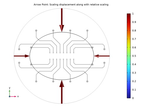
Click to expand the Center of Scaling and Rotation section. In the table, enter the following settings:
Mesh 1
Generate the mesh as follows.
Free Triangular 1
In the Mesh toolbar, click  More Generators and choose Free Triangular.
Size
1
In the Model Builder window, click Size.
2
In the Settings window for Size, locate the Element Size section.
3
From the Predefined list, choose Fine.
Free Triangular 1
1
In the Model Builder window, click Free Triangular 1.
2
In the Settings window for Free Triangular, locate the Boundary Selection section.
3
From the Selection list, choose Cathode.
Size 1
1
Right-click Free Triangular 1 and choose Size.
2
In the Settings window for Size, locate the Element Size section.
3
From the Predefined list, choose Extra fine.
Swept 1
1
In the Mesh toolbar, click  Swept.
2
In the Settings window for Swept, locate the Domain Selection section.
3
From the Geometric entity level list, choose Domain.
4
From the Selection list, choose Electrolyte Swept Mesh Regions.
5
Click to expand the Source Faces section. Click  Paste Selection.
6
In the Paste Selection dialog, type 9 in the Selection text field.
7
8
In the Settings window for Swept, locate the Mesh Generation section.
9
From the Elements list, choose Prisms.
Size 1
1
Right-click Swept 1 and choose Size.
2
In the Settings window for Size, locate the Geometric Entity Selection section.
3
From the Geometric entity level list, choose Boundary.
4
Click  Paste Selection.
5
In the Paste Selection dialog, type 9 in the Selection text field.
6
7
In the Settings window for Size, locate the Element Size section.
8
From the Predefined list, choose Finer.
Distribution 1
1
In the Model Builder window, right-click Swept 1 and choose Distribution.
2
In the Settings window for Distribution, locate the Distribution section.
3
In the Number of elements text field, type 2.
Distribution 2
1
Right-click Swept 1 and choose Distribution.
2
In the Settings window for Distribution, locate the Domain Selection section.
3
From the Selection list, choose Electrolyte Swept Mesh Region 2.
Free Triangular 2
1
In the Mesh toolbar, click  More Generators and choose Free Triangular.
2
Size 1
1
Right-click Free Triangular 2 and choose Size.
2
In the Settings window for Size, locate the Geometric Entity Selection section.
3
From the Geometric entity level list, choose Edge.
4
From the Selection list, choose Transformation Edge.
5
Locate the Element Size section. From the Predefined list, choose Extremely fine.
Swept 2
1
In the Mesh toolbar, click  Swept.
2
In the Settings window for Swept, locate the Domain Selection section.
3
From the Geometric entity level list, choose Domain.
4
From the Selection list, choose Free Shape Domain.
Size 1
1
Right-click Swept 2 and choose Size.
2
In the Settings window for Size, locate the Geometric Entity Selection section.
3
From the Geometric entity level list, choose Boundary.
4
5
Locate the Element Size section. From the Predefined list, choose Extra fine.
Distribution 1
In the Model Builder window, right-click Swept 2 and choose Distribution.
Free Tetrahedral 1
1
In the Mesh toolbar, click  Free Tetrahedral.
2
In the Model Builder window, right-click Mesh 1 and choose Build All.
Study 1
Next, add Shape Optimization study node.
Shape Optimization
1
In the Study toolbar, click  Optimization and choose Shape Optimization.
2
Click  Get Initial Value.
3
In the Model Builder window, click Shape Optimization.
4
In the Settings window for Shape Optimization, locate the Optimization Solver section.
5
In the Move limits text field, type 0.2.
6
Locate the Objective Function section. In the table, enter the following settings:
7
Find the Objective settings subsection. From the Objective scaling list, choose Initial solution based.
8
Click to expand the Output section. From the Keep solutions list, choose First and last.
9
Select the Plot checkbox.
10
11
Click the  Go to XY View button in the Graphics toolbar.
Step 1: Stationary
1
In the Model Builder window, click Step 1: Stationary.
2
In the Settings window for Stationary, locate the Study Settings section.
3
From the Tolerance list, choose User controlled.
4
In the Relative tolerance text field, type 1e-6.
Finally, compute the results.
5
In the Study toolbar, click  Compute.
Results
First, create mirror data sets and then plot the thickness on the cathode copper layout along with the initial aperture and then with the shape-optimized aperture.
Mirror 3D 1
1
In the Model Builder window, expand the Results > Datasets node.
2
Right-click Results > Datasets and choose More 3D Datasets > Mirror 3D.
3
In the Settings window for Mirror 3D, locate the Plane Data section.
4
In the X-coordinate text field, type 9.5.
Mirror 3D 2
1
In the Results toolbar, click  More Datasets and choose Mirror 3D.
2
In the Settings window for Mirror 3D, locate the Data section.
3
From the Dataset list, choose Mirror 3D 1.
4
Locate the Plane Data section. From the Plane list, choose xz-planes.
5
In the y-coordinate text field, type 10.
Thickness on Cathode and Aperture Shapes
1
In the Results toolbar, click  3D Plot Group.
2
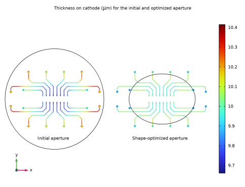
In the Settings window for 3D Plot Group, type Thickness on Cathode and Aperture Shapes in the Label text field.
3
Locate the Data section. From the Dataset list, choose Mirror 3D 2.
4
Click to expand the Title section. From the Title type list, choose Manual.
5
In the Title text area, type Thickness on cathode (\mu m) for the initial and optimized aperture.
6
Clear the Parameter indicator text field.
Surface 1
1
In the Thickness on Cathode and Aperture Shapes toolbar, click  Surface.
2
In the Settings window for Surface, locate the Expression section.
3
In the Expression text field, type thickness_cathode.
4
From the Unit list, choose µm.
Selection 1
1
In the Thickness on Cathode and Aperture Shapes toolbar, click  Selection.
2
In the Settings window for Selection, locate the Selection section.
3
From the Selection list, choose Cathode.
Thickness on Cathode and Aperture Shapes
In the Model Builder window, under Results click Thickness on Cathode and Aperture Shapes.
Line 1
1
In the Thickness on Cathode and Aperture Shapes toolbar, click  Line.
2
In the Settings window for Line, locate the Expression section.
3
In the Expression text field, type 1.
4
Select the Description checkbox. In the associated text field, type Optimized Aperture Shape.
5
Locate the Coloring and Style section. From the Line type list, choose Tube.
6
Select the Radius scale factor checkbox. In the associated text field, type 0.005.
7
From the Coloring list, choose Uniform.
8
From the Color list, choose Black.
Selection 1
1
In the Thickness on Cathode and Aperture Shapes toolbar, click  Selection.
2
In the Settings window for Selection, locate the Selection section.
3
From the Selection list, choose Transformation Edge.
Thickness on Cathode and Aperture Shapes
In the Model Builder window, under Results click Thickness on Cathode and Aperture Shapes.
Annotation 1
1
In the Thickness on Cathode and Aperture Shapes toolbar, click  Annotation.
2
In the Settings window for Annotation, locate the Annotation section.
3
In the Text text field, type Shape-optimized aperture.
4
Locate the Position section. In the x text field, type 8.6.
5
In the y text field, type 9.
6
Locate the Coloring and Style section. Clear the Show point checkbox.
Thickness on Cathode and Aperture Shapes
1
In the Model Builder window, click Thickness on Cathode and Aperture Shapes.
2
In the Settings window for 3D Plot Group, locate the Plot Settings section.
3
Clear the Plot dataset edges checkbox.
Surface 2
1
In the Model Builder window, under Results > Thickness on Cathode and Aperture Shapes right-click Surface 1 and choose Duplicate.
2
In the Settings window for Surface, locate the Data section.
3
From the Dataset list, choose Mirror 3D 2.
4
From the Optimization solution list, choose 0.
5
Click to expand the Title section. From the Title type list, choose None.
6
Click to expand the Inherit Style section. From the Plot list, choose Surface 1.
Transformation 1
1
Right-click Surface 2 and choose Transformation.
2
In the Settings window for Transformation, locate the Transformation section.
3
In the x text field, type -3.
Line 2
1
In the Model Builder window, under Results > Thickness on Cathode and Aperture Shapes right-click Line 1 and choose Duplicate.
2
In the Settings window for Line, locate the Data section.
3
From the Dataset list, choose Mirror 3D 2.
4
From the Optimization solution list, choose 0.
5
Locate the Expression section. In the Description text field, type Initial Aperture Shape.
6
Click to expand the Inherit Style section. From the Plot list, choose Line 1.
Transformation 1
1
Right-click Line 2 and choose Transformation.
2
In the Settings window for Transformation, locate the Transformation section.
3
In the x text field, type -3.
Annotation 2
1
In the Model Builder window, under Results > Thickness on Cathode and Aperture Shapes right-click Annotation 1 and choose Duplicate.
2
In the Settings window for Annotation, locate the Data section.
3
From the Dataset list, choose Mirror 3D 2.
4
From the Optimization solution list, choose 0.
5
Locate the Annotation section. In the Text text field, type Initial aperture.
6
Locate the Position section. In the x text field, type 5.9.
Thickness on Cathode and Aperture Shapes
1
Click the  Go to XY View button in the Graphics toolbar.
2
Click the  Show Grid button in the Graphics toolbar.
3
In the Model Builder window, click Thickness on Cathode and Aperture Shapes.
4
In the Thickness on Cathode and Aperture Shapes toolbar, click  Plot.
Shape Optimization
Next, edit the default Shape Optimization plot which shows the transformation of the aperture from the initial size to the optimized size.
1
In the Model Builder window, click Shape Optimization.
2
In the Settings window for 3D Plot Group, locate the Data section.
3
From the Dataset list, choose Mirror 3D 2.
4
Click to expand the Title section. From the Title type list, choose Manual.
5
In the Title text area, type Arrow Point: Scaling displacement along with relative scaling.
6
Click the  Go to Default View button in the Graphics toolbar.
7
Click the  Go to XY View button in the Graphics toolbar.
8
Click the  Zoom In button in the Graphics toolbar.
Selection 1
1
In the Model Builder window, expand the Shape Optimization node.
2
Right-click Line 1 and choose Selection.
3
In the Settings window for Selection, locate the Selection section.
4
From the Selection list, choose Transformation Edge.
Surface 1
1
In the Model Builder window, right-click Shape Optimization and choose Surface.
2
In the Settings window for Surface, locate the Expression section.
3
In the Expression text field, type 1.
4
Locate the Coloring and Style section. From the Coloring list, choose Uniform.
5
From the Color list, choose Gray.
Selection 1
1
Right-click Surface 1 and choose Selection.
2
In the Settings window for Selection, locate the Selection section.
3
From the Selection list, choose Cathode.
Line 2
1
In the Model Builder window, under Results > Shape Optimization right-click Line 1 and choose Duplicate.
2
In the Model Builder window, click Line 2.
3
In the Settings window for Line, locate the Data section.
4
From the Dataset list, choose Mirror 3D 2.
5
From the Optimization solution list, choose 0.
6
Locate the Coloring and Style section. From the Color list, choose Gray.
Shape Optimization
1
In the Model Builder window, click Shape Optimization.
2
In the Settings window for 3D Plot Group, locate the Plot Settings section.
3
Clear the Plot dataset edges checkbox.
4
In the Shape Optimization toolbar, click  Plot.
Appendix — Geometry Modeling Instructions
From the File menu, choose New.
New
In the New window, click  Model Wizard.
Model Wizard
1
In the Model Wizard window, click  3D.
2
Global Definitions
Parameters 1
1
In the Model Builder window, under Global Definitions click Parameters 1.
2
In the Settings window for Parameters, locate the Parameters section.
3
Click  Load from File.
4
Browse to the model’s Application Libraries folder and double-click the file pcb_aperture_optimization_geom_sequence_parameters.txt.
Geometry 1
1
In the Model Builder window, under Component 1 (comp1) click Geometry 1.
2
In the Settings window for Geometry, locate the Units section.
3
From the Length unit list, choose in.
PCB
1
In the Geometry toolbar, click  Block.
2
In the Settings window for Block, type PCB in the Label text field.
3
Locate the Size and Shape section. In the Width text field, type PCBWidth+2*PCBMargin.
4
In the Depth text field, type PCBHeight+2*PCBMargin.
5
In the Height text field, type PCBThickness.
6
Locate the Position section. In the x text field, type PCBxMin-PCBMargin.
7
In the y text field, type PCByMin-PCBMargin.
8
In the z text field, type PCBOffset-PCBThickness.
9
Locate the Selections of Resulting Entities section. Select the Resulting objects selection checkbox.
10
Click the  Transparency button in the Graphics toolbar.
Work Plane 1 (wp1)
1
In the Geometry toolbar, click  Work Plane.
2
In the Settings window for Work Plane, locate the Plane Definition section.
3
In the z-coordinate text field, type PCBOffset.
4
Locate the Selections of Resulting Entities section. Find the Cumulative selection subsection. Click New.
5
In the New Cumulative Selection dialog, type PCB copper layout in the Name text field.
6
7
In the Settings window for Work Plane, click  Go to Plane Geometry.
Work Plane 1 (wp1) > Import 1 (imp1)
1
In the Home toolbar, click  Import.
2
In the Settings window for Import, locate the Source section.
3
Click  Browse.
4
5
Click  Import.
6
Locate the Layers section. In the table, clear the Import checkbox for Dielectric.
Geometry 1
Work Plane 1 (wp1)
In the Model Builder window, collapse the Component 1 (comp1) > Geometry 1 > Work Plane 1 (wp1) node.
Rim
1
In the Model Builder window, right-click Geometry 1 and choose Selections > Explicit Selection.
2
In the Settings window for Explicit Selection, type Rim in the Label text field.
3
Locate the Entities to Select section. From the Geometric entity level list, choose Boundary.
4
Click the  Zoom Extents button in the Graphics toolbar.
5
On the object wp1, select Boundary 1 only.
6
Click  Build Selected.
Cathode
1
In the Geometry toolbar, click  Selections and choose Difference Selection.
2
In the Settings window for Difference Selection, locate the Geometric Entity Level section.
3
From the Level list, choose Boundary.
4
Locate the Input Entities section. Click the  Add button for Selections to add.
5
In the Add dialog, select PCB copper layout in the Selections to add list.
6
7
In the Settings window for Difference Selection, locate the Input Entities section.
8
Click the  Add button for Selections to subtract.
9
In the Add dialog, select Rim in the Selections to subtract list.
10
11
In the Settings window for Difference Selection, type Cathode in the Label text field.
12
Click  Build Selected.
Bath
1
In the Geometry toolbar, click  Block.
2
In the Settings window for Block, type Bath in the Label text field.
3
Locate the Size and Shape section. In the Width text field, type BathWidth.
4
In the Depth text field, type BathHeight.
5
In the Height text field, type BathDepth.
6
Locate the Position section. In the x text field, type PCBxMin-(BathWidth-PCBWidth)/2.
7
In the y text field, type PCByMin-(BathHeight-PCBHeight)/2.
8
Locate the Selections of Resulting Entities section. Select the Resulting objects selection checkbox.
Electrolyte Swept Mesh Region 1
1
In the Geometry toolbar, click  Block.
2
In the Settings window for Block, type Electrolyte Swept Mesh Region 1 in the Label text field.
3
Locate the Size and Shape section. In the Width text field, type BathWidth.
4
In the Depth text field, type BathHeight.
5
In the Height text field, type PCBThickness.
6
Locate the Position section. In the x text field, type PCBxMin-(BathWidth-PCBWidth)/2.
7
In the y text field, type PCByMin-(BathHeight-PCBHeight)/2.
8
In the z text field, type PCBOffset-PCBThickness.
9
Locate the Selections of Resulting Entities section. Select the Resulting objects selection checkbox.
Work Plane 2 (wp2)
1
In the Geometry toolbar, click  Work Plane.
2
In the Settings window for Work Plane, locate the Plane Definition section.
3
From the Plane type list, choose Face parallel.
4
Click the  Zoom Extents button in the Graphics toolbar.
5
On the object blk2, select Boundary 4 only.
6
Click  Go to Plane Geometry.
Work Plane 2 (wp2) > Rectangle 1 (r1)
1
In the Work Plane toolbar, click  Rectangle.
2
In the Settings window for Rectangle, locate the Size and Shape section.
3
In the Width text field, type BathWidth/6.
4
In the Height text field, type BathHeight.
5
Locate the Position section. In the xw text field, type -BathWidth/2+BathWidth/6/2.
6
In the yw text field, type -BathHeight/2.
Work Plane 2 (wp2) > Array 1 (arr1)
1
In the Work Plane toolbar, click  Transforms and choose Array.
2
Click the  Zoom Extents button in the Graphics toolbar.
3
4
In the Model Builder window, click Array 1 (arr1).
5
In the Settings window for Array, locate the Size section.
6
In the xw size text field, type 3.
7
Locate the Displacement section. In the xw text field, type BathWidth/3.
Geometry 1
Work Plane 2 (wp2)
In the Model Builder window, collapse the Component 1 (comp1) > Geometry 1 > Work Plane 2 (wp2) node.
Anode
1
In the Geometry toolbar, click  Extrude.
2
In the Settings window for Extrude, type Anode in the Label text field.
3
Locate the Distances section. In the table, enter the following settings:
4
Select the Reverse direction checkbox.
5
Locate the Selections of Resulting Entities section. Select the Resulting objects selection checkbox.
6
From the Show in physics list, choose Boundary selection.
Difference 1 (dif1)
1
In the Model Builder window, right-click Geometry 1 and choose Booleans and Partitions > Difference.
2
Select the objects blk2 and blk3 only.
3
In the Settings window for Difference, locate the Difference section.
4
Click to select the  Activate Selection toggle button for Objects to subtract.
5
From the Objects to subtract list, choose PCB.
6
Select the objects blk1 and ext1 only.
Work Plane 3 (wp3)
1
In the Geometry toolbar, click  Work Plane.
2
In the Settings window for Work Plane, locate the Plane Definition section.
3
In the z-coordinate text field, type ApertureOffset+PCBOffset-4*ApertureThickness.
4
Click  Go to Plane Geometry.
Work Plane 3 (wp3) > Cross Section 1 (cro1)
1
In the Work Plane toolbar, click  Cross Section.
2
In the Settings window for Cross Section, locate the Cross Section section.
3
From the Intersect list, choose Selected objects.
4
From the Objects to intersect list, choose Bath.
Geometry 1
Work Plane 3 (wp3)
1
In the Model Builder window, collapse the Component 1 (comp1) > Geometry 1 > Work Plane 3 (wp3) node.
2
In the Model Builder window, click Work Plane 3 (wp3).
3
In the Settings window for Work Plane, click  Build Selected.
Extrude 2 (ext2)
1
In the Model Builder window, right-click Geometry 1 and choose Extrude.
2
In the Settings window for Extrude, locate the Distances section.
3
4
Click  Build Selected.
Aperture Source
1
In the Geometry toolbar, click  Work Plane.
2
In the Settings window for Work Plane, type Aperture Source in the Label text field.
3
Locate the Plane Definition section. In the z-coordinate text field, type ApertureOffset+PCBOffset.
4
Locate the Selections of Resulting Entities section. Select the Resulting objects selection checkbox.
5
Click  Go to Plane Geometry.
Aperture Source (wp4) > Rectangle 1 (r1)
1
In the Work Plane toolbar, click  Rectangle.
2
In the Settings window for Rectangle, locate the Size and Shape section.
3
In the Width text field, type BathWidth.
4
In the Height text field, type BathHeight.
5
Locate the Position section. In the xw text field, type PCBxMin-(BathWidth-PCBWidth)/2.
6
In the yw text field, type PCByMin-(BathHeight-PCBHeight)/2.
Aperture Source (wp4) > Circle 1 (c1)
1
In the Work Plane toolbar, click  Circle.
2
In the Settings window for Circle, locate the Size and Shape section.
3
In the Radius text field, type ApertureRadius.
4
Locate the Position section. In the xw text field, type 9.5.
5
In the yw text field, type 10.
6
Locate the Selections of Resulting Entities section. Select the Resulting objects selection checkbox.
Edges Adjacent to Circle
1
In the Work Plane toolbar, click  Selections and choose Adjacent Selection.
2
In the Settings window for Adjacent Selection, type Edges Adjacent to Circle in the Label text field.
3
Locate the Input Entities section. Click  Add.
4
In the Add dialog, select Circle 1 in the Input selections list.
5
Aperture Source (wp4)
1
In the Model Builder window, collapse the Component 1 (comp1) > Geometry 1 > Aperture Source (wp4) node.
2
In the Model Builder window, click Aperture Source (wp4).
3
In the Settings window for Work Plane, click  Build Selected.
Difference 2 (dif2)
1
In the Geometry toolbar, click  Booleans and Partitions and choose Difference.
2
In the Settings window for Difference, locate the Difference section.
3
Click the  Paste Selection button for Objects to add.
4
In the Paste Selection dialog, type dif1,wp1 in the Selection text field.
5
6
In the Settings window for Difference, locate the Difference section.
7
Click to select the  Activate Selection toggle button for Objects to subtract.
8
Click the  Paste Selection button for Objects to subtract.
9
In the Paste Selection dialog, type ext2,wp4 in the Selection text field.
10
11
In the Settings window for Difference, locate the Difference section.
12
Select the Keep objects to subtract checkbox.
Union 1 (uni1)
1
In the Geometry toolbar, click  Booleans and Partitions and choose Union.
2
In the Settings window for Union, locate the Union section.
3
Click the  Paste Selection button for Input objects.
4
In the Paste Selection dialog, type ext2,wp4 in the Selection text field.
5
Work Plane 5 (wp5)
1
In the Geometry toolbar, click  Work Plane.
2
In the Settings window for Work Plane, locate the Plane Definition section.
3
From the Plane list, choose yz-plane.
4
In the x-coordinate text field, type PCBxMin-(BathWidth-PCBWidth)/2+BathWidth/2.
5
In the Model Builder window, collapse the Work Plane 5 (wp5) node.
Work Plane 6 (wp6)
1
In the Geometry toolbar, click  Work Plane.
2
In the Settings window for Work Plane, locate the Plane Definition section.
3
From the Plane list, choose zx-plane.
4
In the y-coordinate text field, type PCByMin-(BathHeight-PCBHeight)/2+BathHeight/2.
5
In the Model Builder window, collapse the Work Plane 6 (wp6) node.
Partition Domains 1 (pard1)
1
In the Geometry toolbar, click  Booleans and Partitions and choose Partition Domains.
2
In the Settings window for Partition Domains, locate the Partition Domains section.
3
From the Work plane list, choose Work Plane 5 (wp5).
4
On the object dif2, select Domains 1–4 only.
5
On the object uni1, select Domains 1 and 2 only.
6
Locate the Selections of Resulting Entities section. Select the Resulting objects selection checkbox.
7
Click  Build Selected.
Partition Domains 2 (pard2)
1
In the Geometry toolbar, click  Booleans and Partitions and choose Partition Domains.
2
On the object pard1(1), select Domains 1–8 only.
3
On the object pard1(2), select Domains 1–4 only.
4
In the Settings window for Partition Domains, locate the Selections of Resulting Entities section.
5
Select the Resulting objects selection checkbox.
6
Find the Cumulative selection subsection. From the Contribute to list, choose PCB copper layout.
7
Click  Build Selected.
Delete Entities 1 (del1)
1
In the Model Builder window, right-click Geometry 1 and choose Delete Entities.
2
In the Settings window for Delete Entities, locate the Entities or Objects to Delete section.
3
From the Geometric entity level list, choose Domain.
4
Click the  Go to Default View button in the Graphics toolbar.
5
On the object pard2(1), select Domain 8 only.
6
Click the  Zoom Box button in the Graphics toolbar.
7
On the object pard2(1), select Domains 5–8 only.
8
On the object pard2(2), select Domains 3 and 4 only.
9
Click the  Zoom Extents button in the Graphics toolbar.
10
On the object pard2(1), select Domains 4–8 only.
11
On the object pard2(2), select Domains 3 and 4 only.
12
Click the  Zoom Box button in the Graphics toolbar.
13
On the object pard2(1), select Domains 1–8 only.
14
On the object pard2(2), select Domains 1–4 only.
15
Click the  Zoom Extents button in the Graphics toolbar.
16
On the object pard2(1), select Domains 1–8 and 12 only.
17
On the object pard2(2), select Domains 1–4 only.
18
Click the  Zoom Box button in the Graphics toolbar.
19
On the object pard2(1), select Domains 1–12 only.
20
On the object pard2(2), select Domains 1–6 only.
21
Click  Build Selected.
22
Click the  Zoom Extents button in the Graphics toolbar.
Form Union (fin)
1
In the Model Builder window, under Component 1 (comp1) > Geometry 1 click Form Union (fin).
2
In the Settings window for Form Union/Assembly, locate the Form Union/Assembly section.
3
From the Action list, choose Form an assembly.
4
In the Geometry toolbar, click  Build All.
5
Click the  Zoom Extents button in the Graphics toolbar.
Create some selections for use when setting up the model.
Electrolyte Swept Mesh Region 2
1
In the Geometry toolbar, click  Selections and choose Box Selection.
2
In the Settings window for Box Selection, type Electrolyte Swept Mesh Region 2 in the Label text field.
3
Locate the Box Limits section. In the z minimum text field, type 0.
4
In the z maximum text field, type 0.
Electrolyte Swept Mesh Regions
1
In the Geometry toolbar, click  Selections and choose Union Selection.
2
In the Settings window for Union Selection, type Electrolyte Swept Mesh Regions in the Label text field.
3
Locate the Input Entities section. Click  Add.
4
In the Add dialog, in the Selections to add list, choose Electrolyte Swept Mesh Region 1 and Electrolyte Swept Mesh Region 2.
5
6
In the Settings window for Union Selection, click  Build Selected.
Free Shape Domain
1
In the Geometry toolbar, click  Selections and choose Adjacent Selection.
2
In the Settings window for Adjacent Selection, type Free Shape Domain in the Label text field.
3
Locate the Input Entities section. From the Geometric entity level list, choose Boundary.
4
5
In the Add dialog, select Circle 1 (Aperture Source) in the Input selections list.
6
7
In the Settings window for Adjacent Selection, locate the Output Entities section.
8
From the Geometric entity level list, choose Adjacent domains.
Transformation Boundary
1
In the Geometry toolbar, click  Selections and choose Union Selection.
2
In the Settings window for Union Selection, type Transformation Boundary in the Label text field.
3
Locate the Geometric Entity Level section. From the Level list, choose Boundary.
4
Locate the Input Entities section. Click  Add.
5
In the Add dialog, select Circle 1 (Aperture Source) in the Selections to add list.
6
Transformation Edge
1
In the Geometry toolbar, click  Selections and choose Union Selection.
2
In the Settings window for Union Selection, type Transformation Edge in the Label text field.
3
Locate the Geometric Entity Level section. From the Level list, choose Edge.
4
Locate the Input Entities section. Click  Add.
5
In the Add dialog, select Edges Adjacent to Circle (Aperture Source) in the Selections to add list.
6
7
In the Settings window for Union Selection, click  Build Selected.