|
|
|
|
1
|
|
2
|
In the Select Physics tree, select Electrochemistry > Primary and Secondary Current Distribution > Primary Current Distribution (cd).
|
|
3
|
Click Add.
|
|
4
|
Click
|
|
5
|
|
6
|
Click
|
|
1
|
|
2
|
|
3
|
Click
|
|
4
|
|
5
|
Click
|
|
1
|
|
2
|
|
3
|
|
4
|
|
5
|
|
6
|
Click
|
|
1
|
|
2
|
|
3
|
|
4
|
|
5
|
|
6
|
|
7
|
|
8
|
Click
|
|
1
|
|
2
|
Select the object cyl1 only.
|
|
3
|
|
4
|
|
5
|
|
6
|
Click
|
|
1
|
|
2
|
|
3
|
|
1
|
|
2
|
|
3
|
|
4
|
On the object uni1, select Domains 1 and 3–7 only.
|
|
5
|
Click
|
|
1
|
|
2
|
Click in the Graphics window and then press Ctrl+A to select all objects.
|
|
3
|
|
4
|
|
5
|
|
1
|
|
2
|
|
3
|
|
4
|
|
5
|
|
6
|
|
7
|
|
8
|
|
9
|
Clear the Automatic detection of small details checkbox.
|
|
10
|
|
1
|
|
2
|
|
3
|
Click
|
|
4
|
Browse to the model’s Application Libraries folder and double-click the file car_door_parameters.txt.
|
|
1
|
|
2
|
|
3
|
|
5
|
|
1
|
|
2
|
|
3
|
|
5
|
|
1
|
In the Model Builder window, under Component 1 (comp1) > Primary Current Distribution (cd) click Electrolyte 1.
|
|
2
|
|
3
|
|
1
|
|
2
|
|
3
|
|
4
|
|
1
|
|
2
|
|
3
|
|
1
|
|
2
|
|
3
|
|
4
|
|
6
|
Click to expand the Film Resistance section. From the Film resistance list, choose Thickness and conductivity.
|
|
7
|
|
8
|
|
9
|
|
10
|
|
11
|
|
1
|
|
2
|
|
3
|
In the Stoichiometric coefficients for dissolving–depositing species: table, enter the following settings:
|
|
1
|
|
2
|
|
3
|
|
4
|
Click
|
|
5
|
|
1
|
|
2
|
|
3
|
|
4
|
|
1
|
In the Model Builder window, under Results click Electrode Potential with Respect to Adjacent Reference (cd).
|
|
2
|
In the Settings window for 3D Plot Group, type Electrode Potential vs. Adjacent Reference, All Electrodes in the Label text field.
|
|
1
|
|
2
|
In the Settings window for 3D Plot Group, type Electrode Potential vs. Adjacent Reference, Cathode Upside in the Label text field.
|
|
1
|
In the Model Builder window, expand the Electrode Potential vs. Adjacent Reference, Cathode Upside node, then click Surface Slit 1.
|
|
2
|
|
3
|
|
4
|
|
1
|
|
2
|
|
3
|
|
1
|
|
2
|
|
1
|
|
2
|
In the Settings window for 3D Plot Group, type Electrode Potential vs. Adjacent Reference, Cathode Downside in the Label text field.
|
|
1
|
In the Model Builder window, expand the Electrode Potential vs. Adjacent Reference, Cathode Downside node, then click Surface Slit 1.
|
|
2
|
|
3
|
|
4
|
Locate the Expression on the Downside section. In the Expression text field, type root.comp1.cd.Evsrefd.
|
|
5
|
|
1
|
|
2
|
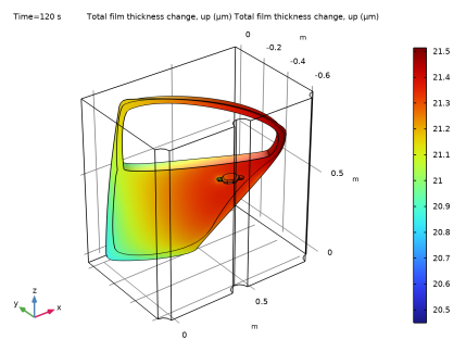
In the Settings window for 3D Plot Group, type Total Film Thickness, Cathode in the Label text field.
|
|
1
|
|
2
|
In the Settings window for 3D Plot Group, type Total Film Thickness, Cathode Upside in the Label text field.
|
|
1
|
In the Model Builder window, expand the Total Film Thickness, Cathode Upside node, then click Surface Slit 1.
|
|
2
|
|
3
|
|
4
|
|
1
|
|
2
|
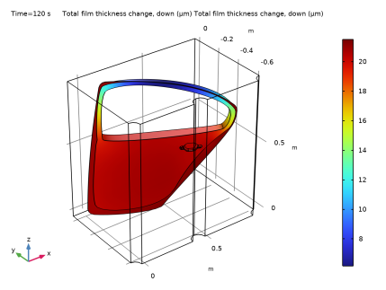
In the Settings window for 3D Plot Group, type Total Film Thickness, Cathode Downside in the Label text field.
|
|
1
|
In the Model Builder window, expand the Total Film Thickness, Cathode Downside node, then click Surface Slit 1.
|
|
2
|
|
3
|
|
4
|
|
1
|
|
2
|
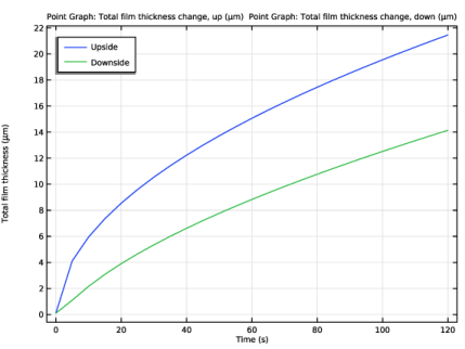
In the Settings window for 1D Plot Group, type Total Film Thickness Comparison in the Label text field.
|
|
3
|
Locate the Plot Settings section.
|
|
4
|
|
1
|
|
3
|
In the Settings window for Point Graph, click Replace Expression in the upper-right corner of the y-Axis Data section. From the menu, choose Component 1 (comp1) > Primary Current Distribution > Dissolving–depositing species > cd.sbtotu - Total film thickness change, up - m.
|
|
4
|
|
5
|
|
6
|
|
1
|
|
2
|
|
3
|
Click to select the
|
|
4
|
Click Replace Expression in the upper-right corner of the y-Axis Data section. From the menu, choose Component 1 (comp1) > Primary Current Distribution > Dissolving–depositing species > cd.sbtotd - Total film thickness change, down - m.
|
|
5
|
Locate the Legends section. In the table, enter the following settings:
|
|
1
|
|
2
|
|
3
|
|
4
|
|
1
|
|
2
|
|
3
|
|
4
|
|
5
|