PDF

Piezoresistive Pressure Sensor — Layered Shell Version
Introduction
Piezoresistive pressure sensors were some of the first MEMS devices to be commercialized. Compared to capacitive pressure sensors, they are simpler to integrate with electronics, their response is more linear, and they are inherently shielded from RF noise. They do, however, usually require more power during operation, and the fundamental noise limits of the sensor are higher than their capacitive counterparts. Historically, piezoresistive devices have been dominant in the pressure sensor market.
This example considers the design of the MPX100 series pressure sensors originally produced by the semiconductor products division of Motorola Inc. (now Freescale Semiconductor Inc.). Although the sensor is no longer in production, a detailed analysis of its design is given in Ref. 1, and an archived data sheet is available from Freescale Semiconductor Inc. (Ref. 2).
This model is a layered shell version of the Piezoresistive Pressure Sensor model in the MEMS Module Application Library and requires the MEMS Module, Structural Mechanics Module, and Composite Materials Module. This tutorial demonstrates how to model piezoresistive effect using the Electric Currents in Layered Shells interface in combination with the Layered Shell interface.
Model Definition
The model consists square membrane with side 1 mm and thickness 20 μm, supported around its edges by region 0.1mm wide, which is intended to represent the remainder of the wafer. The supporting region is fixed on its underside (representing a connection to the thicker handle of the device die). Near to one edge of the membrane an X-shaped piezoresistor (or Xducer™)1 and part of its associated interconnects are visible. The geometry is shown in Figure 1. The base geometry used to set up the layered physics interfaces is shown in Figure 2.
The piezoresistor is assumed to have a uniform p-type dopant density of 1.32×1019 cm3 and a thickness of 400 nm. The interconnects are assumed to have the same thickness but a dopant density of 1.45×1020 cm3. Only a part of the interconnects is included in the geometry, since their conductivity is sufficiently high that they do not contribute to the voltage output of the device.
The edges of the die are aligned with the {110} directions of the silicon. The die edges are also aligned with the global X- and Y-axes in the COMSOL Multiphysics model. The piezoresistor is oriented at 45° to the die edge, and so lies in the [100] direction of the crystal. In the COMSOL Multiphysics model, a rotated coordinate system with an angle of rotation 45° about the global Z-axis is added to define the orientation of the crystal. Later this rotated coordinate system is used to define the first tangent of a boundary coordinate system which is used in the layered material stack.
Figure 1: Scaled 3D geometry of piezoresistive pressure sensor.
Figure 2: The layered shell version of the model geometry.
Figure 3: Zones with different layers in the scaled geometry. The green zone has only n-Silicon layer, the red zone has n-Silicon and p-Silicon layers.
Figure 4: The cross sectional view of zones having layers of different material and thickness.
Device Physics and Equations
The conductivity of the Xducer™ sensor changes when the membrane in its vicinity is subject to an applied stress. This effect is known as the piezoresistance effect and is usually associated with semiconducting materials. In semiconductors, piezoresistance results from the strain-induced alteration of the material’s band structure, and the associated changes in carrier mobility and number density. The relation between the electric field, E, and the current, J, within a piezoresistor is:
(1)
where ρ is the resistivity and Δρ is the induced change in the resistivity. In the general case both ρ and Δρ are rank 2 tensors (matrices). The change in resistance is related to the stress, σ, by the constitutive relationship:
(2)
where Π is the piezoresistance tensor (SI units: Pa1Ωm), a material property. Note that the definition of Π in COMSOL Multiphysics includes the resistivity in each element of the tensor, rather than having a scalar multiple outside of Π (which is possible only for materials with isotropic conductivity). Π is in this case a rank-4 tensor; however, it can be represented as a matrix if the resistivity and stress are converted to vectors within a reduced subscript notation. Within the Voigt notation used by COMSOL Multiphysics for this purpose, Equation 2 becomes:
(3)
The Δρ vector computed from Equation 3 is assembled into matrix form in the following manner in Equation 1:
(4)
Silicon has cubic symmetry, and as a result the Π matrix can be described in terms of three independent constants in the following manner:
For p-type silicon the Π44 constant is two orders of magnitude larger than either the Π11 or the Π12 coefficients. The Π66 element (which is equal in magnitude to the Π44 element) couples the σxy shear stress, with the Δρxy off-diagonal term in the change in resistivity matrix. In turn, Δρxy couples a current in the x direction to an induced electric field in the y direction (and vice versa). This is the principle of the Xducer™ transducer. An applied voltage (typically 3 V; see Ref. 2) across the [100] oriented arm of the X produces a current (typically 6 mA; see Ref. 2) down this arm. Shear stresses are present in the Xducer™ as a result of the pressure induced deformation of the diaphragm in which it is implanted. Through the piezoresistance effect, these shear stresses cause an electric field or potential gradient transverse to the direction of current flow, in the [010] arm of the X. Across the width of the transducer, the potential gradient sums up to produce an induced voltage difference between the [010] arms of the X. According to the device data sheet, under normal operating conditions a 60 mV potential difference is generated from a 100 kPa applied pressure with a 3 V applied bias (Ref. 2).
The situation is complicated somewhat by the detailed current distribution within the device, since the voltage sensing elements increase the width of the current carrying silicon wire locally, leading to a “short circuit” effect (Ref. 3) or a spreading out of the current into the sense arms of the X.
Results and Discussion
Figure 5 shows the displacement of the diaphragm as a result of a 100 kPa pressure difference. At the center of the diaphragm the displacement is 1.25 μm. A simple isotropic model for the deform displacement given in Ref. 1 predicts an order of magnitude value of 4 μm (assuming a Young’s modulus of 170 GPa and a Poisson’s ratio of 0.06). The agreement is reasonable considering the limitations of the analytic model, which is derived by a crude variational guess. A more accurate value for the shear stress in local coordinates at the midpoint of the diaphragm edge is given in Ref. 1 as:
where P is the applied pressure, L is the length of the diaphragm edge, and H is the diaphragm thickness. This equation predicts the magnitude of the local shear stress to be 35 MPa, in good agreement with the minimum value shown in Figure 6, which is also 34.6 MPa. Theoretically the shear stress should be maximal at the midpoint of the edge of the diaphragm. Figure 7 shows the shear stress along the edge in the model. This shows a maximum magnitude at the center of each of the two edges along which the plot is made.
Figure 5: Diaphragm displacement as a result of a 100 kPa applied pressure.
Figure 6: Shear stress, shown in the local coordinate system of the piezoresistor . The shear stress is has its highest magnitude close to the piezoresistor with a value of approximately 34.6 MPa.
Figure 7: Plot of the local shear stress along two edges of the diaphragm.
The output of the model during normal operation shows good agreement with the manufacturer’s data sheet, given that the device dimensions and doping levels have been guessed. With an applied bias of 3 V a typical operating current of 5.9 mA is obtained (compare the current quoted in Ref. 2 of 6 mA). The model produces an output voltage of 52 mV, similar to the actual device output of 60 mV quoted in Ref. 2. The detailed current and voltage distribution within the Xducer™ is shown in Figure 8. There is clear evidence of the current flow “spreading out” into the sense electrodes (which are narrower), a phenomenon described in Ref. 3 as the “short circuit” effect. The asymmetry in the potential, which is induced by the piezoresistive effect, is also apparent in the figure.
Figure 8: Arrows: Current density, Contours: Electric Potential, for a device driven by a 3 V bias with an applied pressure of 100 kPa.
Notes About the COMSOL Implementation
Modeling a composite laminated shell requires a 2D surface geometry, called a base surface, and a Layered Material node that adds an extra dimension (1D) to the base surface geometry in the surface normal direction. Using the Layered Material functionality, you can model several layers of different thicknesses, material properties, and fiber orientations. You can optionally specify the interface materials between the layers and the control mesh elements in each layer.
The Layered Material Stack node is used to define various zones/sections of the piezoresistive pressure sensor.
The third direction for the selected coordinate system in the Single Layer Material, Layered Material Link, or Layered Material Stack represents the normal direction of the Layered Shell or Shell physics. This is also the direction in which the layer stacking is interpreted from bottom to top, and therefore, it is crucial to know it during modeling. There are two ways to achieve this:
-
Using physics symbols: Go to the physics settings, find the Physics Symbols section, and select the Enable physics symbols checkbox. Then go to the material feature, for instance, Linear Elastic Material, to see the normal direction represented by green arrows in the geometry.
-
To visualize the results as a 3D solid object, you can use the Layered Material dataset, which creates a virtual 3D solid object combining the surface geometry (2D) and the extra dimension (1D).
References
1. S.D. Senturia, “A Piezoresistive Pressure Sensor,” Microsystem Design, chapter 18, Springer, 2000.
2. Motorola Semiconductor MPX100 series technical data, document: MPX100/D, 1998 (available from Freescale Semiconductor Inc at www.nxp.com).
3. M. Bao, Analysis and Design Principles of MEMS Devices, Elsevier B.V., 2005.
Application Library path: Composite_Materials_Module/Multiphysics/piezoresistive_pressure_sensor_layered
Modeling Instructions
From the File menu, choose New.
New
In the New window, click  Model Wizard.
Model Wizard
1
In the Model Wizard window, click  3D.
2
In the Select Physics tree, select Structural Mechanics > Electromagnetics–Structure Interaction > Piezoresistivity > Piezoresistivity, Layered Shell.
3
Click Add.
4
Click  Study.
5
In the Select Study tree, select General Studies > Stationary.
6
Geometry 1
For convenience, the device geometry is inserted from an existing file.
The dimensions of this geometry are given in micrometers, so you need to change the length unit accordingly.
1
In the Model Builder window, under Component 1 (comp1) click Geometry 1.
2
In the Settings window for Geometry, locate the Units section.
3
From the Length unit list, choose µm.
4
In the Geometry toolbar, click Insert Sequence and choose Insert Sequence.
5
Browse to the model’s Application Libraries folder and double-click the file piezoresistive_pressure_sensor_shell_geom_sequence.mph.
6
In the Geometry toolbar, click  Build All.
7
Click the  Zoom Extents button in the Graphics toolbar.
Some selections in the inserted geometry need to be modified for the current model setup.
Model Boundaries (unisel1)
In the Model Builder window, under Component 1 (comp1) > Geometry 1 right-click Model Boundaries (unisel1) and choose Delete.
Model Boundaries
1
In the Geometry toolbar, click  Selections and choose Explicit Selection.
2
In the Settings window for Explicit Selection, type Model Boundaries in the Label text field.
3
Locate the Entities to Select section. From the Geometric entity level list, choose Boundary.
4
Select the Group by continuous tangent checkbox.
5
On the object ige2, select Boundaries 1–18 only.
6
Drag and drop below Membrane (boxsel1).
7
Click  Build Selected.
Fixed Edges (adjsel1)
In the Model Builder window, right-click Fixed Edges (adjsel1) and choose Delete.
Fixed Boundaries (difsel1)
1
In the Settings window for Difference Selection, locate the Input Entities section.
2
Click Build Preceding State.
3
Click the  Add button for Selections to add.
4
In the Add dialog, select Model Boundaries in the Selections to add list.
5
6
In the Settings window for Difference Selection, click  Build Selected.
Definitions
Rotated System 2 (sys2)
1
In the Definitions toolbar, click  Coordinate Systems and choose Rotated System.
2
In the Settings window for Rotated System, locate the Rotation section.
3
Find the Euler angles subsection. In the α text field, type -45[deg].
Setup the first axis of the boundary coordinate system from the rotated system.
Boundary System 1 (sys1)
1
In the Model Builder window, click Boundary System 1 (sys1).
2
In the Settings window for Boundary System, locate the Settings section.
3
Find the Coordinate names subsection. From the Create first tangent direction from list, choose Rotated System 2 (sys2).
4
From the Axis list, choose x1.
Add Material
1
In the Materials toolbar, click  Add Material to open the Add Material window.
2
Go to the Add Material window.
3
In the tree, select Piezoresistivity > n-Silicon (single-crystal, lightly doped).
4
Click the Add to Global Materials button in the window toolbar.
5
In the tree, select Piezoresistivity > p-Silicon (single-crystal, lightly doped).
6
Click the Add to Global Materials button in the window toolbar.
7
In the Materials toolbar, click  Add Material to close the Add Material window.
Materials
Layered Material Stack 1 (stlmat1)
In the Model Builder window, under Component 1 (comp1) right-click Materials and choose Layers > Layered Material Stack.
Layered Material Link 1 (stlmat1.stllmat1)
In the Model Builder window, under Component 1 (comp1) > Materials > Layered Material Stack 1 (stlmat1) right-click Layered Material Link 1 (stlmat1.stllmat1) and choose Delete.
Layered Material Stack 1 (stlmat1)
1
In the Settings window for Layered Material Stack, locate the Orientation and Position section.
2
From the Position list, choose Bottom side on boundary.
n-Silicon
1
Right-click Layered Material Stack 1 (stlmat1) and choose Layered Material.
2
In the Settings window for Layered Material, type n-Silicon in the Label text field.
3
Locate the Layer Definition section. In the table, enter the following settings:
p-Silicon
1
Right-click Layered Material Stack 1 (stlmat1) and choose Layered Material.
2
In the Settings window for Layered Material, type p-Silicon in the Label text field.
3
Locate the Boundary Selection section. From the Selection list, choose Electric currents.
4
Locate the Layer Definition section. In the table, enter the following settings:
Layered Material Stack 1 (stlmat1)
1
In the Model Builder window, click Layered Material Stack 1 (stlmat1).
2
In the Settings window for Layered Material Stack, click Layer Cross-Section Preview in the upper-right corner of the Layered Material Settings section. From the menu, choose Create Layer Cross-Section Plot.
Layered Shell (lshell)
Linear Elastic Material 1
1
In the Model Builder window, expand the Results node, then click Component 1 (comp1) > Layered Shell (lshell) > Linear Elastic Material 1.
2
In the Settings window for Linear Elastic Material, locate the Linear Elastic Material section.
3
From the Material symmetry list, choose Anisotropic.
4
From the Material data ordering list, choose Voigt (11, 22, 33, 23, 13, 12).
Fixed Constraint, Interface 1
1
In the Physics toolbar, click  Boundaries and choose Fixed Constraint, Interface.
2
In the Settings window for Fixed Constraint, Interface, locate the Boundary Selection section.
3
From the Selection list, choose Fixed Boundaries.
4
Locate the Interface Selection section. From the Apply to list, choose Bottom interface.
Face Load 1
1
In the Physics toolbar, click  Boundaries and choose Face Load.
2
In the Settings window for Face Load, locate the Interface Selection section.
3
From the Apply to list, choose Top interface.
4
Locate the Force section. From the Load type list, choose Pressure.
5
In the p text field, type 100[kPa].
6
Locate the Boundary Selection section. From the Selection list, choose Membrane.
Continuity 1
1
In the Physics toolbar, click  Edges and choose Continuity.
2
In the Settings window for Continuity, locate the Layer Selection section.
3
From the Source list, choose Layered Material Stack 1 (stlmat1.zone1).
4
From the Destination list, choose Layered Material Stack 1 (stlmat1.zone2).
Electric Currents in Layered Shells (ecis)
1
In the Model Builder window, under Component 1 (comp1) click Electric Currents in Layered Shells (ecis).
2
In the Settings window for Electric Currents in Layered Shells, locate the Boundary Selection section.
3
From the Selection list, choose Electric currents.
4
Locate the Shell Properties section. Clear the Use all layers checkbox.
5
In the Selection table, clear the checkbox for Layer 1 - n-Silicon.
The electric conductivity is a function of number density. To change default value of number density, activate the Model Input sections in the Conductive Shell 1 and Piezoresistive Shell 1 features.
6
Click the  Show More Options button in the Model Builder toolbar.
7
In the Show More Options dialog, in the tree, select the checkbox for the node Physics > Advanced Physics Options.
8
Click OK to show model input sections.
Conductive Shell 1
1
In the Model Builder window, under Component 1 (comp1) > Electric Currents in Layered Shells (ecis) click Conductive Shell 1.
2
In the Settings window for Conductive Shell, click to expand the Model Input section.
3
In the nd text field, type 1.45e20[1/cm^3].
Piezoresistive Shell 1
1
In the Model Builder window, click Piezoresistive Shell 1.
2
In the Settings window for Piezoresistive Shell, locate the Boundary Selection section.
3
From the Selection list, choose Piezoresistor.
4
Click to expand the Model Input section. In the nd text field, type 1.32e19[1/cm^3].
Conductive Shell 1
In the Model Builder window, click Conductive Shell 1.
Terminal 1
1
In the Physics toolbar, click  Attributes and choose Terminal.
2
In the Settings window for Terminal, locate the Edge Selection section.
3
Click  Clear Selection.
4
5
Locate the Terminal section. From the Terminal type list, choose Voltage.
6
In the V0 text field, type 3.
Conductive Shell 1
In the Model Builder window, click Conductive Shell 1.
Terminal 2
1
In the Physics toolbar, click  Attributes and choose Terminal.
2
In the Settings window for Terminal, locate the Edge Selection section.
3
Click  Clear Selection.
4
Conductive Shell 1
In the Model Builder window, click Conductive Shell 1.
Terminal 3
1
In the Physics toolbar, click  Attributes and choose Terminal.
2
In the Settings window for Terminal, locate the Edge Selection section.
3
Click  Clear Selection.
4
Ground 1
1
In the Physics toolbar, click  Edges and choose Ground.
2
In the Settings window for Ground, locate the Edge Selection section.
3
Click  Clear Selection.
4
Mesh 1
1
In the Model Builder window, under Component 1 (comp1) click Mesh 1.
2
In the Settings window for Mesh, locate the Sequence Type section.
3
From the list, choose User-controlled mesh.
Size
1
In the Model Builder window, under Component 1 (comp1) > Mesh 1 click Size.
2
In the Settings window for Size, locate the Element Size Parameters section.
3
In the Maximum element size text field, type 60.
4
In the Minimum element size text field, type 0.5.
Size 1
1
Right-click Size and choose Duplicate.
2
In the Settings window for Size, locate the Geometric Entity Selection section.
3
From the Geometric entity level list, choose Boundary.
4
From the Selection list, choose Piezoresistor.
5
Locate the Element Size Parameters section. In the Maximum element size text field, type 2.
6
In the Minimum element size text field, type 0.1.
Size 2
1
Right-click Size 1 and choose Duplicate.
2
In the Settings window for Size, locate the Geometric Entity Selection section.
3
From the Selection list, choose Connections.
4
Locate the Element Size Parameters section. In the Maximum element size text field, type 6.
Size 3
1
Right-click Size 2 and choose Duplicate.
2
In the Settings window for Size, locate the Geometric Entity Selection section.
3
From the Geometric entity level list, choose Edge.
4
5
Locate the Element Size Parameters section. In the Maximum element size text field, type 0.4.
Free Triangular 1
1
In the Model Builder window, right-click Free Triangular 1 and choose Move Down three times.
2
In the Settings window for Free Triangular, locate the Boundary Selection section.
3
From the Selection list, choose All boundaries.
4
Click  Build All.
Study 1
Switch off the generation of default plots in the study. We will use Result Templates.
1
In the Model Builder window, click Study 1.
2
In the Settings window for Study, locate the Study Settings section.
3
Clear the Generate default plots checkbox.
4
In the Study toolbar, click  Compute.
Set default units for result presentation.
Results
Preferred Units 1
1
In the Results toolbar, click  Configurations and choose Preferred Units.
2
In the Settings window for Preferred Units, locate the Units section.
3
Click  Add Physical Quantity.
4
In the Physical Quantity dialog, select Solid Mechanics > Stress tensor (N/m^2) in the tree.
5
6
In the Settings window for Preferred Units, locate the Units section.
7
8
Click  Apply.
Now create a dataset for the detailed current and voltage distribution plots.
Study 1/Solution 1 (2) (sol1)
1
In the Model Builder window, expand the Results > Datasets node.
2
Right-click Results > Datasets > Study 1/Solution 1 (sol1) and choose Duplicate.
Selection
1
In the Results toolbar, click  Attributes and choose Selection.
2
In the Settings window for Selection, locate the Geometric Entity Selection section.
3
From the Geometric entity level list, choose Boundary.
4
From the Selection list, choose Electric currents.
Layered Material 1
1
In the Results toolbar, click  More Datasets and choose Layered Material.
2
In the Settings window for Layered Material, locate the Data section.
3
From the Dataset list, choose Study 1/Solution 1 (2) (sol1).
Use the result templates to show the von Mises stress, displacement and voltage distribution.
Result Templates
1
In the Home toolbar, click  Windows and choose Result Templates.
2
Go to the Result Templates window.
3
In the tree, select Study 1/Solution 1 (1) (sol1) > Layered Shell > von Mises Stress (lshell).
4
Click the Add Result Template button in the window toolbar.
5
In the tree, select Study 1/Solution 1 (1) (sol1) > Layered Shell > Displacement (lshell).
6
Click the Add Result Template button in the window toolbar.
7
In the tree, select Study 1/Solution 1 (1) (sol1) > Electric Currents in Layered Shells > Electric Potential (ecis).
8
Click the Add Result Template button in the window toolbar.
9
In the Results toolbar, click  Result Templates to close the Result Templates window.
Results
von Mises Stress (lshell)
1
In the Settings window for 3D Plot Group, locate the Color Legend section.
2
Select the Show maximum and minimum values checkbox.
Surface 1
1
In the Model Builder window, expand the von Mises Stress (lshell) node, then click Surface 1.
2
In the von Mises Stress (lshell) toolbar, click  Plot.
Displacement (lshell)
1
In the Model Builder window, under Results click Displacement (lshell).
2
In the Settings window for 3D Plot Group, locate the Color Legend section.
3
Select the Show maximum and minimum values checkbox.
4
In the Displacement (lshell) toolbar, click  Plot.
Electric Potential (ecis)
1
In the Model Builder window, click Electric Potential (ecis).
2
In the Settings window for 3D Plot Group, locate the Data section.
3
From the Dataset list, choose Layered Material 1.
4
Locate the Plot Settings section. From the View list, choose New view.
5
In the Electric Potential (ecis) toolbar, click  Plot.
Now create a plot of the shear stress in the local coordinate system of the piezoresistor.
In-Plane Shear Stress
1
In the Results toolbar, click  3D Plot Group.
2
In the Settings window for 3D Plot Group, type In-Plane Shear Stress in the Label text field.
3
Locate the Data section. From the Dataset list, choose Layered Material.
4
Locate the Color Legend section. Select the Show maximum and minimum values checkbox.
Surface 1
1
Right-click In-Plane Shear Stress and choose Surface.
2
In the Settings window for Surface, locate the Expression section.
3
In the Expression text field, type lshell.slGp12.
4
In the In-Plane Shear Stress toolbar, click  Plot.
Create a line plot of the shear stress in the local coordinate system of the piezoresistor.
In-Plane Shear Stress along Diaphragm Edges
1
In the Results toolbar, click  1D Plot Group.
2
In the Settings window for 1D Plot Group, type In-Plane Shear Stress along Diaphragm Edges in the Label text field.
3
Click to expand the Title section. From the Title type list, choose Label.
4
Locate the Plot Settings section.
5
Select the y-axis label checkbox. In the associated text field, type Stress tensor, local coordinate system, 12-component (MPa).
Line Graph 1
1
Right-click In-Plane Shear Stress along Diaphragm Edges and choose Line Graph.
2
3
In the Settings window for Line Graph, locate the y-Axis Data section.
4
In the Expression text field, type side(2,lshell.atxd1(lshell.d,lshell.slGp12)).
5
From the Unit list, choose MPa.
6
In the In-Plane Shear Stress along Diaphragm Edges toolbar, click  Plot.
Now create a plot of the detailed current and voltage distribution.
Current and Voltage
1
In the Home toolbar, click  Add Plot Group and choose 3D Plot Group.
2
In the Settings window for 3D Plot Group, type Current and Voltage in the Label text field.
3
Locate the Data section. From the Dataset list, choose Study 1/Solution 1 (2) (sol1).
4
Locate the Plot Settings section. From the View list, choose New view.
Contour 1
1
Right-click Current and Voltage and choose Contour.
2
In the Settings window for Contour, locate the Expression section.
3
In the Expression text field, type V.
4
Locate the Levels section. In the Total levels text field, type 20.
5
Locate the Coloring and Style section. From the Contour type list, choose Tube.
6
Select the Radius scale factor checkbox.
7
In the Tube radius expression text field, type 1.
8
In the Radius scale factor text field, type 0.07.
9
From the Color table list, choose ThermalDark.
10
From the Color table transformation list, choose Reverse.
Arrow Surface 1
1
In the Model Builder window, right-click Current and Voltage and choose Arrow Surface.
2
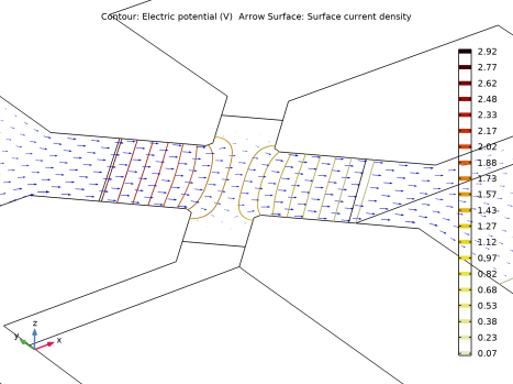
In the Settings window for Arrow Surface, click Replace Expression in the upper-right corner of the Expression section. From the menu, choose Component 1 (comp1) > Electric Currents in Layered Shells > Currents and charge > ecis.JsX,...,ecis.JsZ - Surface current density (material and geometry frames).
3
Locate the Expression section.
4
Select the Description checkbox. In the associated text field, type Surface current density.
5
Locate the Coloring and Style section.
6
Select the Scale factor checkbox. In the associated text field, type 0.005.
7
Locate the Arrow Positioning section. In the Number of arrows text field, type 3000.
8
Locate the Coloring and Style section. From the Color list, choose Blue.
9
In the Current and Voltage toolbar, click  Plot.
Result Templates
1
In the Results toolbar, click  Result Templates to open the Result Templates window.
2
Go to the Result Templates window.
3
In the tree, select Study 1/Solution 1 (1) (sol1) > Layered Shell > Geometry and Layup (lshell) > Shell Geometry (lshell).
4
Click the Add Result Template button in the window toolbar.
5
In the Results toolbar, click  Result Templates to close the Result Templates window.
Results
Shell Geometry (lshell)
Click the  Go to Default View button in the Graphics toolbar.
Layered Material 2 (Shell Geometry)
1
In the Model Builder window, under Results > Datasets click Layered Material 2 (Shell Geometry).
2
In the Settings window for Layered Material, locate the Layers section.
3
In the Scale text field, type 5.
Shell Geometry (lshell)
1
In the Model Builder window, under Results click Shell Geometry (lshell).
2
In the Shell Geometry (lshell) toolbar, click  Plot.
Stack Zones
1
Right-click Shell Geometry (lshell) and choose Duplicate.
2
In the Settings window for 3D Plot Group, type Stack Zones in the Label text field.
3
Locate the Data section. From the Dataset list, choose Layered Material 2 (Shell Geometry).
Surface 1
1
In the Model Builder window, expand the Stack Zones node, then click Surface 1.
2
In the Settings window for Surface, locate the Expression section.
3
In the Expression text field, type stlmat1.zone.
4
Locate the Coloring and Style section. From the Coloring list, choose Color table.
5
From the Color table list, choose TrafficLight.
Stack Zones
1
In the Model Builder window, click Stack Zones.
2
In the Stack Zones toolbar, click  Plot.
3
Drag and drop below Layer Cross-Section Preview.
Appendix — Geometry Modeling Instructions
From the File menu, choose New.
New
In the New window, click  Blank Model.
Add Component
In the Home toolbar, click  Add Component and choose 3D.
Geometry 1
1
In the Settings window for Geometry, locate the Units section.
2
From the Length unit list, choose µm.
Work Plane 1 (wp1)
In the Geometry toolbar, click  Work Plane.
Work Plane 1 (wp1) > Plane Geometry
In the Model Builder window, click Plane Geometry.
Work Plane 1 (wp1) > Square 1 (sq1)
1
In the Work Plane toolbar, click  Square.
2
In the Settings window for Square, locate the Size section.
3
In the Side length text field, type 1200.
4
Locate the Position section. From the Base list, choose Center.
5
In the yw text field, type 478.
6
Click to expand the Layers section. In the table, enter the following settings:
7
Select the Layers to the left checkbox.
8
Select the Layers to the right checkbox.
9
Select the Layers on top checkbox.
Work Plane 1 (wp1) > Square 2 (sq2)
1
In the Work Plane toolbar, click  Square.
2
In the Settings window for Square, locate the Size section.
3
In the Side length text field, type 22.6.
4
Locate the Position section. From the Base list, choose Center.
Work Plane 1 (wp1) > Rectangle 1 (r1)
1
In the Work Plane toolbar, click  Rectangle.
2
In the Settings window for Rectangle, locate the Size and Shape section.
3
In the Width text field, type 52.5.
4
In the Height text field, type 10.
5
Locate the Position section. From the Base list, choose Center.
6
Locate the Rotation Angle section. In the Rotation text field, type 45.
7
Click to expand the Layers section. In the table, enter the following settings:
8
Select the Layers to the right checkbox.
9
Select the Layers to the left checkbox.
10
Clear the Layers on bottom checkbox.
Work Plane 1 (wp1) > Rectangle 2 (r2)
1
Right-click Component 1 (comp1) > Geometry 1 > Work Plane 1 (wp1) > Plane Geometry > Rectangle 1 (r1) and choose Duplicate.
2
In the Settings window for Rectangle, locate the Size and Shape section.
3
In the Width text field, type 62.5.
4
In the Height text field, type 20.
5
Locate the Rotation Angle section. In the Rotation text field, type -45.
6
Locate the Layers section. In the table, enter the following settings:
Work Plane 1 (wp1) > Rectangle 3 (r3)
1
In the Work Plane toolbar, click  Rectangle.
2
In the Settings window for Rectangle, locate the Size and Shape section.
3
In the Width text field, type 210.
4
In the Height text field, type 140.
5
Locate the Position section. From the Base list, choose Center.
6
In the yw text field, type -15.
Work Plane 1 (wp1) > Rectangle 4 (r4)
1
In the Work Plane toolbar, click  Rectangle.
2
In the Settings window for Rectangle, locate the Size and Shape section.
3
In the Width text field, type 40.
4
In the Height text field, type 50.
5
Locate the Position section. In the xw text field, type -105.
6
In the yw text field, type -35.
Work Plane 1 (wp1) > Rectangle 5 (r5)
1
In the Work Plane toolbar, click  Rectangle.
2
In the Settings window for Rectangle, locate the Size and Shape section.
3
In the Width text field, type 90.
4
In the Height text field, type 40.
5
Locate the Position section. In the xw text field, type -105.
6
In the yw text field, type 15.
Work Plane 1 (wp1) > Rectangle 6 (r6)
1
In the Work Plane toolbar, click  Rectangle.
2
In the Settings window for Rectangle, locate the Size and Shape section.
3
In the Width text field, type 90.
4
In the Height text field, type 40.
5
Locate the Position section. In the xw text field, type -105.
6
In the yw text field, type -85.
Work Plane 1 (wp1) > Rectangle 7 (r7)
1
In the Work Plane toolbar, click  Rectangle.
2
In the Settings window for Rectangle, locate the Size and Shape section.
3
In the Width text field, type 40.
4
In the Height text field, type 30.
5
Locate the Position section. In the xw text field, type -55.
6
In the yw text field, type -45.
Work Plane 1 (wp1) > Mirror 1 (mir1)
1
In the Work Plane toolbar, click  Transforms and choose Mirror.
2
Select the objects r4, r5, r6, and r7 only.
3
In the Settings window for Mirror, locate the Input section.
4
Select the Keep input objects checkbox.
Form Composite Faces 1 (cmf1)
1
In the Model Builder window, under Component 1 (comp1) > Geometry 1 right-click Work Plane 1 (wp1) and choose Virtual Operations > Form Composite Faces.
2
On the object fin, select Boundaries 19, 20, 26–35, and 38 only.
Form Composite Faces 2 (cmf2)
1
In the Geometry toolbar, click  Virtual Operations and choose Form Composite Faces.
2
On the object cmf1, select Boundaries 11, 14–18, 25, 27, and 32–35 only.
Ignore Edges 1 (ige1)
1
In the Geometry toolbar, click  Virtual Operations and choose Ignore Edges.
2
On the object cmf2, select Edges 24 and 94 only.
3
In the Settings window for Ignore Edges, locate the Input section.
4
Clear the Ignore adjacent vertices checkbox.
Form Composite Faces 3 (cmf3)
1
In the Geometry toolbar, click  Virtual Operations and choose Form Composite Faces.
2
On the object ige1, select Boundaries 7, 12, 15, 17, 21, and 24–26 only.
Ignore Edges 2 (ige2)
1
In the Geometry toolbar, click  Virtual Operations and choose Ignore Edges.
2
On the object cmf3, select Edges 4, 6, 8, 12, 84, and 87–89 only.
Piezoresistor
1
In the Geometry toolbar, click  Selections and choose Explicit Selection.
2
In the Settings window for Explicit Selection, type Piezoresistor in the Label text field.
3
Locate the Entities to Select section. From the Geometric entity level list, choose Boundary.
4
On the object ige2, select Boundary 9 only.
Connections
1
In the Geometry toolbar, click  Selections and choose Explicit Selection.
2
In the Settings window for Explicit Selection, type Connections in the Label text field.
3
Locate the Entities to Select section. From the Geometric entity level list, choose Boundary.
4
On the object ige2, select Boundaries 3, 5, 6, 8, 13–15, and 18 only.
Membrane
1
In the Geometry toolbar, click  Selections and choose Box Selection.
2
In the Settings window for Box Selection, type Membrane in the Label text field.
3
Locate the Geometric Entity Level section. From the Level list, choose Boundary.
4
Locate the Box Limits section. In the x minimum text field, type -501.
5
In the x maximum text field, type 501.
6
In the y minimum text field, type -30.
7
In the y maximum text field, type 1000.
8
Locate the Output Entities section. From the Include entity if list, choose Entity inside box.
Model Boundaries
1
In the Geometry toolbar, click  Selections and choose Union Selection.
2
In the Settings window for Union Selection, type Model Boundaries in the Label text field.
3
Locate the Geometric Entity Level section. From the Level list, choose Boundary.
4
Locate the Input Entities section. Click  Add.
5
In the Add dialog, in the Selections to add list, choose Connections and Membrane.
6
Electric currents
1
In the Geometry toolbar, click  Selections and choose Union Selection.
2
In the Settings window for Union Selection, type Electric currents in the Label text field.
3
Locate the Geometric Entity Level section. From the Level list, choose Boundary.
4
Locate the Input Entities section. Click  Add.
5
In the Add dialog, in the Selections to add list, choose Piezoresistor and Connections.
6
Fixed Edges
1
In the Geometry toolbar, click  Selections and choose Adjacent Selection.
2
In the Settings window for Adjacent Selection, type Fixed Edges in the Label text field.
3
Locate the Input Entities section. From the Geometric entity level list, choose Boundary.
4
5
In the Add dialog, select Membrane in the Input selections list.
6
7
In the Settings window for Adjacent Selection, locate the Output Entities section.
8
From the Geometric entity level list, choose Adjacent edges.
Fixed Boundaries
1
In the Geometry toolbar, click  Selections and choose Difference Selection.
2
In the Settings window for Difference Selection, type Fixed Boundaries in the Label text field.
3
Locate the Geometric Entity Level section. From the Level list, choose Boundary.
4
Locate the Input Entities section. Click the  Add button for Selections to add.
5
In the Add dialog, select Model Boundaries in the Selections to add list.
6
7
In the Settings window for Difference Selection, locate the Input Entities section.
8
Click the  Add button for Selections to subtract.
9
In the Add dialog, select Membrane in the Selections to subtract list.
10

1
Xducer™ is believed to be a trademark of Freescale Semiconductor, Inc. f/k/a Motorola, Inc. Neither Freescale Semiconductor Inc. nor Motorola, Inc. has in any way provided any sponsorship or endorsement of, nor do they have any connection or involvement with, COMSOL Multiphysics® software or this model.