
|
|
|
|
|
|
E [GPa]
|
α [1/K]
|
k [W/(m·K)]
|
ρ [kg/m3]
|
Cp [J/(kg·K)]
|
||
|
•
|
Modeling a composite laminate as a layered shell requires a surface geometry, in general referred to as a base surface, and a Layered Material node which adds an extra dimension (1D) to the base surface geometry in the surface normal direction. You can use the Layered Material functionality to model several layers stacked on top of each other having different thicknesses, material properties, and fiber orientations. You can optionally specify the interface materials between the layers, and control the number of through-thickness mesh elements for each layer.
|
|
•
|
The third direction for the selected coordinate system in the Single Layer Material, Layered Material Link, or Layered Material Stack represents the normal direction of the Layered Shell or Shell physics. This is also the direction in which the layer stacking is interpreted from bottom to top, and therefore, it is crucial to know it during modeling. There are two ways to achieve this:
|
|
-
|
Using physics symbols: Go to the physics settings, find the Physics Symbols section, and select the Enable physics symbols checkbox. Then go to the material feature, for instance, Linear Elastic Material, to see the normal direction represented by green arrows in the geometry.
|
|
-
|
Using result templates: When a solution dataset is available, use the result template Thickness and Orientation to plot the normal direction.
|
|
•
|
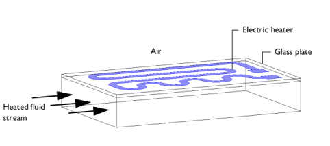
The Thermal Stress, Layered Shell multiphysics interface includes the Heat Transfer in Shell and the Layered Shell interfaces. In the silica glass, these two interfaces solve for temperature and displacements, respectively. In the conducting layer representing the circuit, the temperature, electric potential, and displacement are solved by Heat Transfer in Shell, Electric Currents in Layered Shells, and the Layered Shell interfaces.
|
|
1
|
|
2
|
In the Select Physics tree, select Structural Mechanics > Thermal–Structure Interaction > Thermal Stress, Layered Shell.
|
|
3
|
Click Add.
|
|
4
|
In the Select Physics tree, select AC/DC > Electric Fields and Currents > Electric Currents in Layered Shells (ecis).
|
|
5
|
Click Add.
|
|
6
|
Click
|
|
7
|
|
8
|
Click
|
|
1
|
|
2
|
|
3
|
Click
|
|
4
|
Browse to the model’s Application Libraries folder and double-click the file heating_circuit_layered_parameters.txt.
|
|
1
|
|
2
|
|
3
|
|
1
|
|
2
|
|
1
|
|
2
|
|
3
|
|
4
|
|
5
|
|
6
|
Click
|
|
1
|
Right-click Component 1 (comp1) > Geometry 1 > Work Plane 1 (wp1) > Plane Geometry > Square 1 (sq1) and choose Duplicate.
|
|
2
|
|
3
|
|
4
|
|
5
|
Click
|
|
1
|
|
2
|
|
3
|
|
4
|
Click
|
|
5
|
Browse to the model’s Application Libraries folder and double-click the file heating_circuit_layered_polygon.txt.
|
|
6
|
Click
|
|
1
|
|
2
|
On the object pol1, select Points 2–8, 23–29, 34, 36, 37, 41, and 42 only.
|
|
3
|
|
4
|
|
5
|
Click
|
|
1
|
|
2
|
On the object fil1, select Points 6–12, 26–31, 37, 40, 43, 46, 49, and 50 only.
|
|
3
|
|
4
|
|
5
|
Click
|
|
1
|
|
2
|
|
3
|
|
4
|
|
1
|
|
2
|
Go to the Add Material window.
|
|
3
|
|
4
|
Right-click and choose Add to Global Materials.
|
|
5
|
|
1
|
|
2
|
|
3
|
|
4
|
Click OK.
|
|
1
|
|
2
|
|
3
|
|
4
|
Click OK.
|
|
1
|
|
2
|
|
1
|
|
2
|
|
3
|
Locate the Layer Definition section. In the table, enter the following settings:
|
|
1
|
|
2
|
|
3
|
|
4
|
Click
|
|
5
|
|
6
|
Click OK.
|
|
7
|
|
1
|
|
2
|
|
3
|
|
4
|
Click
|
|
5
|
|
6
|
Click OK.
|
|
7
|
|
1
|
|
2
|
In the Settings window for Layered Material Stack, click Layer Cross-Section Preview in the upper-right corner of the Layered Material Settings section. From the menu, choose Create Layer Cross-Section Plot.
|
|
1
|
|
2
|
|
1
|
In the Model Builder window, under Component 1 (comp1) > Layered Shell (lshell) click Linear Elastic Material 1.
|
|
2
|
|
3
|
|
1
|
|
2
|
|
3
|
|
4
|
|
1
|
|
2
|
|
3
|
|
4
|
|
1
|
|
2
|
|
3
|
|
4
|
|
5
|
In the Selection table, enter the following settings:
|
|
1
|
|
2
|
|
3
|
|
4
|
|
5
|
|
6
|
|
8
|
|
10
|
|
1
|
In the Model Builder window, under Component 1 (comp1) > Heat Transfer in Shells (htlsh) click Solid 1.
|
|
2
|
|
3
|
Clear the Layerwise constant properties checkbox.
|
|
1
|
|
2
|
|
3
|
|
4
|
|
5
|
|
6
|
|
7
|
|
1
|
|
2
|
|
3
|
|
4
|
|
5
|
|
6
|
|
7
|
|
1
|
|
2
|
|
3
|
|
4
|
|
1
|
|
2
|
|
3
|
|
4
|
|
1
|
|
2
|
|
3
|
|
4
|
|
5
|
In the Selection table, enter the following settings:
|
|
1
|
In the Model Builder window, under Component 1 (comp1) click Electric Currents in Layered Shells (ecis).
|
|
2
|
In the Settings window for Electric Currents in Layered Shells, locate the Boundary Selection section.
|
|
3
|
In the list box, select 1 (stlmat1).
|
|
4
|
Click
|
|
6
|
|
7
|
|
1
|
|
3
|
|
4
|
|
1
|
|
3
|
|
4
|
|
5
|
|
1
|
|
2
|
|
3
|
|
4
|
|
5
|
In the Selection table, enter the following settings:
|
|
1
|
|
2
|
|
1
|
|
2
|
|
1
|
|
2
|
|
3
|
|
1
|
|
2
|
|
4
|
Click
|
|
6
|
|
7
|
Locate the Element Size Parameters section.
|
|
8
|
|
9
|
Click
|
|
1
|
|
2
|
|
3
|
Clear the Generate default plots checkbox.
|
|
4
|
|
1
|
|
2
|
|
3
|
Click
|
|
4
|
|
5
|
Click OK.
|
|
6
|
|
8
|
Click
|
|
9
|
|
10
|
Click OK.
|
|
11
|
|
13
|
Select the Apply conversions to expressions with the same dimensions checkbox.
|
|
14
|
Click
|
|
1
|
|
2
|
Go to the Result Templates window.
|
|
3
|
|
4
|
Click the Add Result Template button in the window toolbar.
|
|
5
|
|
6
|
Click the Add Result Template button in the window toolbar.
|
|
1
|
|
2
|
|
1
|
|
2
|
|
3
|
|
4
|
|
1
|
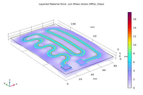
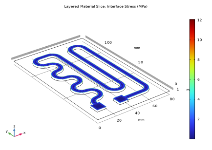
In the Model Builder window, expand the Stress, Glass (lshell) node, then click Layered Material Slice 1.
|
|
2
|
|
3
|
|
4
|
|
5
|
|
6
|
|
1
|
|
2
|
|
3
|
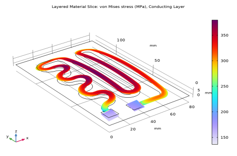
In the Settings window for 3D Plot Group, type Stress, Conducting Layer (lshell) in the Label text field.
|
|
4
|
Locate the Title section. In the Title text area, type Layered Material Slice: von Mises stress (MPa), Conducting Layer.
|
|
1
|
|
2
|
|
3
|
|
4
|
|
1
|
Go to the Result Templates window.
|
|
2
|
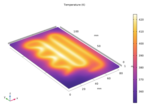
In the tree, select Study 1/Solution 1 (sol1) > Heat Transfer in Shells > Temperature, Shell (htlsh).
|
|
3
|
Click the Add Result Template button in the window toolbar.
|
|
4
|
In the tree, select Study 1/Solution 1 (sol1) > Electric Currents in Layered Shells > Electric Potential (ecis).
|
|
5
|
Click the Add Result Template button in the window toolbar.
|
|
6
|
|
1
|
|
2
|
|
1
|
|
2
|
|
3
|
|
4
|
|
1
|
Go to the Result Templates window.
|
|
2
|
In the tree, select Study 1/Solution 1 (sol1) > Layered Shell > Geometry and Layup (lshell) > Shell Geometry (lshell).
|
|
3
|
Click the Add Result Template button in the window toolbar.
|
|
4
|
|
1
|
|
2
|
|
3
|
|
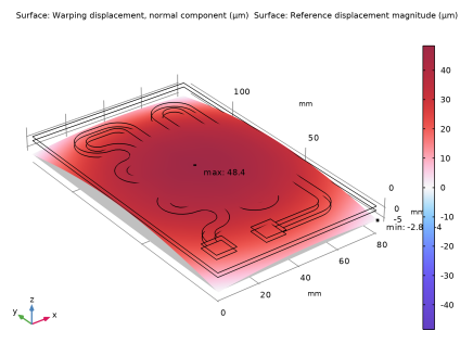
1
|
|
2
|
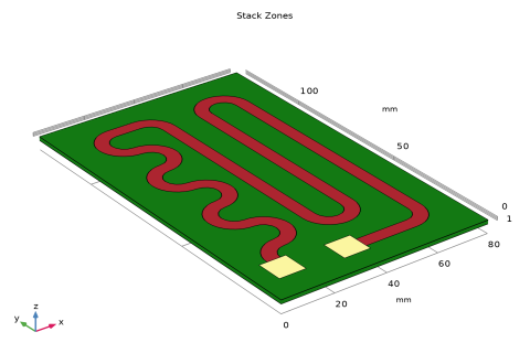
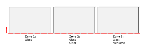
In the Settings window for Surface, click Replace Expression in the upper-right corner of the Expression section. From the menu, choose Component 1 (comp1) > Layered materials > Layered Material Stack 1 (stlmat1) > stlmat1.zone - Zone index - 1.
|
|
3
|
|
4
|
|
5
|
|
1
|
|
2
|
|
1
|
|
2
|
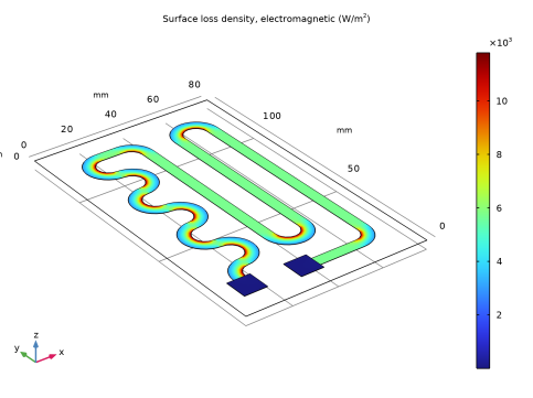
In the Settings window for Surface, click Replace Expression in the upper-right corner of the Expression section. From the menu, choose Component 1 (comp1) > Electric Currents in Layered Shells > Heating and losses > ecis.Qsh - Surface loss density, electromagnetic - W/m².
|
|
3
|
|
1
|
|
2
|
|
3
|
|
4
|
|
1
|
|
2
|
|
3
|
|
4
|
|
5
|
|
1
|
|
3
|
|
1
|
|
2
|
Go to the Result Templates window.
|
|
3
|
|
4
|
Click the Add Result Template button in the window toolbar.
|
|
5
|
|
1
|
|
2
|
|
3
|
|
4
|
|
1
|
|
2
|
|
3
|
|
1
|
|
3
|
|
4
|
|
5
|
|
6
|
Click Replace Expression in the upper-right corner of the Expressions section. From the menu, choose Component 1 (comp1) > Electric Currents in Layered Shells > Heating and losses > ecis.Qsh - Surface loss density, electromagnetic - W/m².
|
|
7
|
|
1
|
|
2
|
In the Settings window for Evaluation Group, type Total Heat Transferred to Fluid in the Label text field.
|
|
3
|
|
1
|
|
2
|
|
3
|
|
4
|
Click Replace Expression in the upper-right corner of the Expressions section. From the menu, choose Component 1 (comp1) > Heat Transfer in Shells > Boundary fluxes > htlsh.hfi2.q0 - Boundary convective heat flux - W/m².
|
|
5
|