PDF

Aluminum Nitride Lamb Wave Resonator — Layered Shell Version
Introduction
This tutorial demonstrates how to model an aluminum nitride Lamb wave resonator using the Electric Currents in Layered Shells interface in combination with the Layered Shell interface. The Lamb wave resonator (LWR) is an important building block in circuits used in mobile communication systems. Its operational characteristics are controlled by the piezoelectric material properties, the pattern of thin conducting layer on its surface, and its dimensions. Using the Piezoeletricity, Layered Shell multiphysics interface and materials from the Piezoelectric Material Library, you can create a digital prototype of an LWR.
This model is a layered shell version of Aluminum Nitride Lamb Wave Resonator — 3D from the MEMS Module Application Library and requires the MEMS Module, Structural Mechanics Module, and Composite Materials Module.
Model Definition
In this tutorial, the LWR is an aluminum nitride (piezoelectric) block with an interdigitated electrode (IDE) on its surface, as shown in Figure 1. The base geometry used to set up the layered physics interfaces is shown in Figure 2. Suspended from four anchor points, the 0.4 μm piezoelectric block responds to AC excitation through the platinum IDE (80 nm). The LWR is designed to resonate at 7.9809 GHz.
The LWR geometric parameters are summarized in the first table in the Modeling Instructions section so the geometry can easily be modified for design optimization. The geometry is rebuilt automatically when geometric parameters are changed if the rules are followed. For example, n must be chosen so that (n+1)/4 is an integer, or = {3, 7, 11, …}. Also, the overlap parameter op should be smaller than the length of the finger l, that is, op < l. Keep in mind, however, that changes in the geometry will shift the resonant frequency. An outline of the steps in the fabrication of an actual LWR can be found in Ref. 1.
In this model, the fully coupled structural and electrostatic equations are solved in the piezoelectric and conducting domain. The model also includes mechanical loss through an isotropic structural loss factor of 0.002 for the piezoelectric and the platinum layers.
In this tutorial we are interested in the symmetric S0 mode, which, in typical applications, results in maximal electromechanical coupling efficiency. Because of the symmetry of the device structure and the symmetry of the S0 mode, only one half of the device needs to be modeled. This reduces computational time, which is important because this model requires a fine mesh to compute accurate eigenmodes.
This tutorial shows the setup of Eigenfrequency and Frequency Domain studies. In the Eigenfrequency study you investigate the eigenmodes of the structure to find the S0 mode. In the subsequent Frequency Domain study, a 1 V drive signal is applied to the signal electrode and the resonator’s frequency response from 7.95 to 8.05 GHz is analyzed.
The results of this example is compared with the solid model variant Aluminum Nitride Lamb Wave Resonator — 3D. To match the results, the model setup needs to be the same. In the solid version of the example, the thin Platinum layer is not modeled explicitly in the Electrostatic interface, rather this thin layer modeled as a layer with either constant voltage or zero voltage using the Terminal and Ground features. In the current example, the thin layer is considered as a conducting layer with uniform or zero voltage across all interfaces using the similar boundary conditions.
In the solid version of example, the Solid Mechanics interface has quadratic Serendipity discretization with three mesh elements across the thickness of the piezoelectric layer, and linear discretization with single mesh element across the conducting layer (through Thin Layer feature). While the Electrostatic interface has quadratic Lagrange discretization. In this example, the quadratic-linear discretization is chosen for the Layered Shell interface, and quadratic discretization for the Electric Currents in Layered Shells interface. Three mesh elements are used in the piezoelectric layer, while only one mesh element is used in the conducting layer. This is specified using the settings of Layered Material nodes.
Figure 1: The 3D geometry of one half of the Lamb wave resonator.
Figure 2: The layered shell version of the model geometry.
Figure 3: Zones with different layers in the layered shell geometry. The red zone has only aluminum nitride, the green zone has aluminum nitride and platinum layers.
Figure 4: Cross-sectional view of zones having layers of different material and thickness.
Results and Discussion
Figure 5 shows the displacement in the z direction for the S0 mode at 7.9809 GHz. In high-frequency resonant devices such as LWRs, the Eigenfrequency study returns many extraneous solutions very close to the mode of interest. Only through visual inspection, one can distinguish the correct mode from the spurious modes. Figure 6 shows the solid displacement across the XZ cut plane through the center of the resonator to verify the S0 mode.
Figure 5: Displacement along the z-axis for the S0 mode at 7.7506 GHz.
Figure 6: Solid displacement across the XZ cut plane through the center of the resonator for the S0 mode at 7.9809 GHz.
Figure 7 shows a log plot of the admittance magnitude versus frequency from 7.95 to 8.05 GHz. The plot is annotated with the positions of resonance and anti-resonance peaks for the calculation of the electromechanical coupling coefficient.
Figure 7: Admittance versus frequency.
The frequency response yields important information relating to the device performance such as the effective electromechanical coupling coefficient given by
where fs and fp are the resonance and anti-resonance frequencies, respectively, with fs = 7.98, fp = 8.03, and kt2 = 1.526%. The effective electromechanical coupling coefficient is known to be a measure of the transduction efficiency for conversion of electrical into mechanical energy.
Notes About the COMSOL Implementation
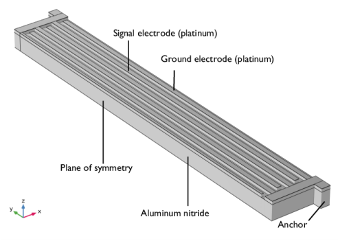
Modeling a composite laminated shell requires a 2D surface geometry, called a base surface, and a Layered Material node that adds an extra dimension (1D) to the base surface geometry in the surface normal direction. Using the Layered Material functionality, you can model several layers of different thicknesses, material properties, and fiber orientations. You can optionally specify the interface materials between the layers and the control mesh elements in each layer.
The Layered Material Stack node is used to define various zones/sections of the Lamb wave resonator.
The third direction for the selected coordinate system in the Single Layer Material, Layered Material Link, or Layered Material Stack represents the normal direction of the Layered Shell or Shell physics. This is also the direction in which the layer stacking is interpreted from bottom to top, and therefore, it is crucial to know it during modeling. There are two ways to achieve this:
-
Using physics symbols: Go to the physics settings, find the Physics Symbols section, and select the Enable physics symbols checkbox. Then go to the material feature, for instance, Linear Elastic Material, to see the normal direction represented by green arrows in the geometry.
-
Reference
1. J. Zou, C.M. Lin, A. Gao, and A.P. Pisano, “The Multi-Mode Resonance in AlN Lamb Wave Resonators,” J. Microelectromech. Syst., vol. 27, no. 6, pp. 973–84, 2018.
Application Library path: Composite_Materials_Module/Multiphysics/aln_lamb_wave_resonator_layered
Modeling Instructions
From the File menu, choose New.
New
In the New window, click  Model Wizard.
Model Wizard
1
In the Model Wizard window, click  3D.
Start by creating a new 3D model with a Piezoelectricity, Layered Shell multiphysics interface.
2
In the Select Physics tree, select Structural Mechanics > Electromagnetics–Structure Interaction > Piezoelectricity > Piezoelectricity, Layered Shell.
3
Click Add.
4
Click  Study.
5
In the Select Study tree, select Preset Studies for Selected Multiphysics > Eigenfrequency.
6
Geometry 1
Use microns as the geometry unit.
1
In the Model Builder window, under Component 1 (comp1) click Geometry 1.
2
In the Settings window for Geometry, locate the Units section.
3
From the Length unit list, choose µm.
Define and specify the parameters of the model.
Global Definitions
Parameters 1
1
In the Model Builder window, under Global Definitions click Parameters 1.
2
In the Settings window for Parameters, locate the Parameters section.
3
Add material models and layered materials under Global Definitions node.
Add Material
1
In the Materials toolbar, click  Add Material to open the Add Material window.
2
Go to the Add Material window.
3
In the tree, select MEMS > Metals > Pt - Platinum.
4
Click the Add to Global Materials button in the window toolbar.
5
In the tree, select Piezoelectric > Aluminum Nitride.
6
Click the Add to Global Materials button in the window toolbar.
7
In the Materials toolbar, click  Add Material to close the Add Material window.
Global Definitions
Pt - Platinum (mat1)
1
In the Model Builder window, under Global Definitions > Materials click Pt - Platinum (mat1).
2
In the Settings window for Material, click to expand the Material Properties section.
3
In the Material properties tree, select Basic Properties > Isotropic Structural Loss Factor.
4
Click  Add to Material.
5
Locate the Material Contents section. In the table, enter the following settings:
6
Locate the Material Properties section. In the Material properties tree, select Basic Properties > Relative Permittivity.
7
Click  Add to Material.
8
Locate the Material Contents section. In the table, enter the following settings:
Layered Material: Platinum
1
In the Model Builder window, right-click Materials and choose Layered Material.
2
In the Settings window for Layered Material, type Layered Material: Platinum in the Label text field.
3
Locate the Layer Definition section. In the table, enter the following settings:
Layered Material: Aluminum Nitride
1
Right-click Materials and choose Layered Material.
2
In the Settings window for Layered Material, type Layered Material: Aluminum Nitride in the Label text field.
3
Locate the Layer Definition section. In the table, enter the following settings:
Aluminum Nitride (mat2)
1
In the Model Builder window, click Aluminum Nitride (mat2).
2
In the Settings window for Material, locate the Material Properties section.
3
In the Material properties tree, select Basic Properties > Isotropic Structural Loss Factor.
4
Click  Add to Material.
5
Locate the Material Contents section. In the table, enter the following settings:
Create the geometry model for half part of the lamb wave resonator.
Geometry 1
Work Plane 1 (wp1)
1
In the Model Builder window, expand the Component 1 (comp1) > Geometry 1 node.
2
Right-click Geometry 1 and choose Work Plane.
Work Plane 1 (wp1) > Rectangle 1 (r1)
1
In the Work Plane toolbar, click  Rectangle.
2
In the Settings window for Rectangle, locate the Size and Shape section.
3
In the Width text field, type wf.
4
In the Height text field, type l.
5
Locate the Position section. From the Base list, choose Center.
6
In the yw text field, type dy/2.
Work Plane 1 (wp1) > Array 1 (arr1)
1
In the Work Plane toolbar, click  Transforms and choose Array.
2
3
In the Settings window for Array, locate the Size section.
4
In the xw size text field, type (n+1)/4.
5
Locate the Displacement section. In the xw text field, type 4*wf.
Work Plane 1 (wp1) > Move 1 (mov1)
1
In the Work Plane toolbar, click  Transforms and choose Move.
2
Click the  Select All button in the Graphics toolbar.
3
In the Settings window for Move, locate the Input section.
4
Select the Keep input objects checkbox.
5
Locate the Displacement section. In the xw text field, type 2*wf.
6
In the yw text field, type -dy.
Work Plane 1 (wp1) > Rectangle 2 (r2)
1
In the Work Plane toolbar, click  Rectangle.
2
In the Settings window for Rectangle, locate the Size and Shape section.
3
In the Width text field, type (n-1/2)*wf+we.
4
In the Height text field, type 2*wf.
5
Locate the Position section. In the yw text field, type (l+dy)/2.
Work Plane 1 (wp1) > Rectangle 3 (r3)
1
In the Work Plane toolbar, click  Rectangle.
2
In the Settings window for Rectangle, locate the Size and Shape section.
3
In the Width text field, type 2*we.
4
In the Height text field, type la.
5
Locate the Position section. In the xw text field, type (n-1/2)*wf-we.
6
In the yw text field, type (l+dy)/2+2*wf.
Work Plane 1 (wp1) > Mirror 1 (mir1)
1
In the Work Plane toolbar, click  Transforms and choose Mirror.
2
Select the objects r2 and r3 only.
3
In the Settings window for Mirror, locate the Input section.
4
Select the Keep input objects checkbox.
5
Locate the Normal Vector to Line of Reflection section. In the xw text field, type 0.
6
In the yw text field, type -1.
Work Plane 1 (wp1) > Rectangle 4 (r4)
1
In the Work Plane toolbar, click  Rectangle.
2
In the Settings window for Rectangle, locate the Size and Shape section.
3
In the Width text field, type (n+1/2)*wf.
4
In the Height text field, type l+dy.
5
Locate the Position section. From the Base list, choose Center.
6
In the xw text field, type (n+1/2)*wf/2.
Work Plane 1 (wp1) > Partition Objects 1 (par1)
1
In the Work Plane toolbar, click  Booleans and Partitions and choose Partition Objects.
2
Select the object arr1(1,1) only.
3
In the Settings window for Partition Objects, locate the Partition Objects section.
4
Click to select the  Activate Selection toggle button for Tool objects.
5
6
Select the Keep tool objects checkbox.
Work Plane 1 (wp1) > Delete Entities 1 (del1)
1
In the Model Builder window, right-click Plane Geometry and choose Delete Entities.
2
In the Settings window for Delete Entities, locate the Entities or Objects to Delete section.
3
From the Geometric entity level list, choose Domain.
4
On the object par1, select Domain 1 only.
5
Click  Build Selected.
6
In the Model Builder window, right-click Geometry 1 and choose Build All.
7
Click the  Zoom Extents button in the Graphics toolbar.
Define selections for the electrodes and other boundaries. This will make specifying the material models and physics interface settings easier.
Definitions
Signal
1
In the Model Builder window, expand the Component 1 (comp1) > Definitions node.
2
Right-click Definitions and choose Selections > Box.
3
In the Settings window for Box, type Signal in the Label text field.
4
Locate the Geometric Entity Level section. From the Level list, choose Boundary.
5
Locate the Box Limits section. In the y minimum text field, type -l/2.
6
In the z minimum text field, type 0.
7
Locate the Output Entities section. From the Include entity if list, choose Entity inside box.
Ground
1
Right-click Signal and choose Duplicate.
2
In the Settings window for Box, type Ground in the Label text field.
3
Locate the Box Limits section. In the y minimum text field, type -Inf.
4
In the y maximum text field, type l/2.
Electrodes
1
In the Definitions toolbar, click  Union.
2
In the Settings window for Union, type Electrodes in the Label text field.
3
Locate the Geometric Entity Level section. From the Level list, choose Boundary.
4
Locate the Input Entities section. Under Selections to add, click  Add.
5
In the Add dialog, in the Selections to add list, choose Signal and Ground.
6
Symmetry
1
In the Definitions toolbar, click  Box.
2
In the Settings window for Box, type Symmetry in the Label text field.
3
Locate the Geometric Entity Level section. From the Level list, choose Edge.
4
Locate the Box Limits section. In the x maximum text field, type 0.
5
Locate the Output Entities section. From the Include entity if list, choose Entity inside box.
Base Surface
1
In the Definitions toolbar, click  Box.
2
In the Settings window for Box, type Base Surface in the Label text field.
3
Locate the Geometric Entity Level section. From the Level list, choose Boundary.
4
Locate the Box Limits section. In the z minimum text field, type 0.
5
Locate the Output Entities section. From the Include entity if list, choose Entity inside box.
Device
1
In the Definitions toolbar, click  Box.
2
In the Settings window for Box, type Device in the Label text field.
3
Locate the Geometric Entity Level section. From the Level list, choose Boundary.
4
Locate the Box Limits section. In the y minimum text field, type -((l+dy)/2+2*wf+la)+0.01.
5
In the y maximum text field, type (l+dy)/2+2*wf+la-0.01.
Fixed Constraints
1
In the Definitions toolbar, click  Explicit.
2
In the Settings window for Explicit, type Fixed Constraints in the Label text field.
3
Locate the Input Entities section. From the Geometric entity level list, choose Edge.
4
Click  Paste Selection.
5
In the Paste Selection dialog, type 33 40 in the Selection text field.
6
The stacking of the Platinum layer is not the same across the Aluminum Nitride base. In order to model the stacking, add a Layered Material Stack node with Layered Material Link subnodes having different selections.
Materials
Layered Material Stack 1 (stlmat1)
1
In the Model Builder window, under Component 1 (comp1) right-click Materials and choose Layers > Layered Material Stack.
2
In the Settings window for Layered Material Stack, locate the Orientation and Position section.
3
From the Position list, choose Bottom side on boundary.
Aluminum Nitride
1
In the Model Builder window, under Component 1 (comp1) > Materials > Layered Material Stack 1 (stlmat1) click Layered Material Link 1 (stlmat1.stllmat1).
2
In the Settings window for Layered Material Link, type Aluminum Nitride in the Label text field.
3
Locate the Link Settings section. From the Material list, choose Layered Material: Aluminum Nitride (lmat2).
Pt - Platinum
1
In the Model Builder window, right-click Layered Material Stack 1 (stlmat1) and choose Layered Material Link.
2
In the Settings window for Layered Material Link, type Pt - Platinum in the Label text field.
3
Locate the Boundary Selection section. From the Selection list, choose Electrodes.
To visualize the stacking, create a Layer Cross Section Preview plot through an action button in the Layered Material Settings section.
Layered Material Stack 1 (stlmat1)
1
In the Model Builder window, click Layered Material Stack 1 (stlmat1).
2
In the Settings window for Layered Material Stack, click Layer Cross-Section Preview in the upper-right corner of the Layered Material Settings section. From the menu, choose Create Layer Cross-Section Plot.
Results
Layer Cross-Section Preview
1
In the Model Builder window, expand the Results node, then click Layer Cross-Section Preview.
2
In the Layer Cross-Section Preview toolbar, click  Plot.
Specify the settings for the Layered Shell interface.
Layered Shell (lshell)
Linear Elastic Material 1
In the Model Builder window, under Component 1 (comp1) > Layered Shell (lshell) click Linear Elastic Material 1.
Damping 1
1
In the Physics toolbar, click  Attributes and choose Damping.
2
In the Settings window for Damping, locate the Damping Settings section.
3
From the Damping type list, choose Isotropic loss factor.
Piezoelectric Material 1
1
In the Model Builder window, under Component 1 (comp1) > Layered Shell (lshell) click Piezoelectric Material 1.
2
In the Settings window for Piezoelectric Material, locate the Shell Properties section.
3
Clear the Use all layers checkbox.
4
In the Selection table, clear the checkbox for Layer 1 - Pt - Platinum.
Mechanical Damping 1
1
In the Physics toolbar, click  Attributes and choose Mechanical Damping.
2
In the Settings window for Mechanical Damping, locate the Damping Settings section.
3
From the Damping type list, choose Isotropic loss factor.
Fixed Constraint 1
1
In the Physics toolbar, click  Edges and choose Fixed Constraint.
2
In the Settings window for Fixed Constraint, locate the Edge Selection section.
3
From the Selection list, choose Fixed Constraints.
Symmetry 1
1
In the Physics toolbar, click  Edges and choose Symmetry.
2
In the Settings window for Symmetry, locate the Edge Selection section.
3
From the Selection list, choose Symmetry.
Continuity 1
1
In the Physics toolbar, click  Edges and choose Continuity.
2
In the Settings window for Continuity, locate the Layer Selection section.
3
From the Source list, choose Layered Material Stack 1 (stlmat1.zone1).
4
From the Destination list, choose Layered Material Stack 1 (stlmat1.zone2).
5
In the Model Builder window, click Layered Shell (lshell).
6
In the Settings window for Layered Shell, click to expand the Discretization section.
7
From the Displacement field list, choose Quadratic-linear serendipity.
Specify the settings for the Electric Currents in Layered Shells interface.
Electric Currents in Layered Shells (ecis)
Conductive Shell 1
In the Model Builder window, under Component 1 (comp1) > Electric Currents in Layered Shells (ecis) click Conductive Shell 1.
Ground 1
1
In the Physics toolbar, click  Boundaries and choose Ground.
2
In the Settings window for Ground, locate the Boundary Selection section.
3
From the Selection list, choose Ground.
4
Locate the Interface Selection section. From the Apply to list, choose All interfaces.
Conductive Shell 1
In the Model Builder window, click Conductive Shell 1.
Interface Terminal 1
1
In the Physics toolbar, click  Attributes and choose Interface Terminal.
2
In the Settings window for Interface Terminal, locate the Boundary Selection section.
3
From the Selection list, choose Signal.
4
Locate the Interface Selection section. From the Apply to list, choose All interfaces.
5
Locate the Terminal section. From the Terminal type list, choose Voltage.
6
In the V0 text field, type Vapp.
Piezoelectric Layer 1
1
In the Model Builder window, under Component 1 (comp1) > Electric Currents in Layered Shells (ecis) click Piezoelectric Layer 1.
2
In the Settings window for Piezoelectric Layer, locate the Shell Properties section.
3
Clear the Use all layers checkbox.
4
In the Selection table, clear the checkbox for Layer 1 - Pt - Platinum.
Electric Continuity 1
1
In the Physics toolbar, click  Edges and choose Electric Continuity.
2
In the Settings window for Electric Continuity, locate the Layer Selection section.
3
From the Source list, choose Layered Material Stack 1 (stlmat1).
4
From the Destination list, choose Layered Material Stack 1 (stlmat1.zone2).
5
From the Source list, choose Layered Material Stack 1 (stlmat1.zone1).
6
In the Selection table, enter the following settings:
Create the mesh for the model.
Mesh 1
Free Quad 1
1
In the Mesh toolbar, click  More Generators and choose Free Quad.
2
In the Settings window for Free Quad, locate the Boundary Selection section.
3
From the Selection list, choose Base Surface.
Size 1
1
Right-click Free Quad 1 and choose Size.
2
In the Settings window for Size, locate the Element Size section.
3
Click the Custom button.
4
Locate the Element Size Parameters section.
5
Select the Maximum element size checkbox. In the associated text field, type 0.1.
6
Click  Build Selected.
Set up an Eigenfrequency study to search for an eigenfrequency around 8 GHz.
Eigenfrequency
1
In the Model Builder window, click Study 1.
2
In the Settings window for Study, type Eigenfrequency in the Label text field.
3
Locate the Study Settings section. Clear the Generate default plots checkbox.
Step 1: Eigenfrequency
1
In the Model Builder window, under Eigenfrequency click Step 1: Eigenfrequency.
2
In the Settings window for Eigenfrequency, locate the Study Settings section.
3
Select the Desired number of eigenfrequencies checkbox. In the associated text field, type 20.
4
From the Unit list, choose GHz.
5
In the Search for eigenfrequencies around shift text field, type 8.
Solution 1 (sol1)
1
In the Study toolbar, click  Show Default Solver.
2
In the Model Builder window, expand the Solution 1 (sol1) node, then click Eigenvalue Solver 1.
3
In the Settings window for Eigenvalue Solver, locate the Output section.
4
From the Scaling of eigenvectors list, choose Mass matrix.
5
In the Study toolbar, click  Compute.
Add a Layered Material dataset and a Mirror dataset. This dataset will be used to plot the result of the Eigenfrequency study.
Results
Layered Material 1
1
In the Model Builder window, expand the Results > Datasets node.
2
Right-click Results > Datasets and choose More Datasets > Layered Material.
Mirror 3D 1
1
In the Results toolbar, click  More Datasets and choose Mirror 3D.
2
In the Settings window for Mirror 3D, locate the Data section.
3
From the Dataset list, choose Layered Material 1.
4
With the solution from the Eigenfrequency study, create a 3D plot to display the shape of the eigenmode at 8 GHz. Use the Mirror dataset previously created.
Mode Shape
1
In the Results toolbar, click  3D Plot Group.
2
In the Settings window for 3D Plot Group, type Mode Shape in the Label text field.
3
Locate the Data section. From the Dataset list, choose Mirror 3D 1.
4
Locate the Plot Settings section. Clear the Plot dataset edges checkbox.
5
From the View list, choose New view.
6
Locate the Color Legend section. Clear the Show legends checkbox.
Surface 1
1
Right-click Mode Shape and choose Surface.
2
In the Settings window for Surface, locate the Expression section.
3
In the Expression text field, type w.
4
Select the Description checkbox.
5
Click to expand the Range section. Select the Manual color range checkbox.
6
In the Minimum text field, type -1E10.
7
In the Maximum text field, type 1E10.
8
In the Mode Shape toolbar, click  Plot.
9
Click the  Go to XY View button in the Graphics toolbar.
10
Click the  Go to XY View button in the Graphics toolbar.
11
Click the  Go to XY View button in the Graphics toolbar.
12
Click the  Show Grid button in the Graphics toolbar.
With the solution from the Eigenfrequency study, create a Slice plot to display the eigenmode in the xz cut plane through the center.
Mode Shape, Center XZ Plane
1
In the Results toolbar, click  3D Plot Group.
2
In the Settings window for 3D Plot Group, type Mode Shape, Center XZ Plane in the Label text field.
3
Locate the Data section. From the Dataset list, choose Mirror 3D 1.
4
Locate the Plot Settings section. From the View list, choose New view.
5
Locate the Color Legend section. Clear the Show legends checkbox.
Slice 1
1
Right-click Mode Shape, Center XZ Plane and choose Slice.
2
In the Settings window for Slice, locate the Expression section.
3
Select the Description checkbox.
4
Locate the Plane Data section. From the Plane list, choose zx-planes.
5
In the Planes text field, type 1.
6
Locate the Coloring and Style section. From the Color table type list, choose Discrete.
7
In the Number of bands text field, type 15.
Mode Shape, Center XZ Plane
1
In the Model Builder window, click Mode Shape, Center XZ Plane.
2
In the Settings window for 3D Plot Group, locate the Plot Settings section.
3
Clear the Plot dataset edges checkbox.
4
In the Mode Shape, Center XZ Plane toolbar, click  Plot.
5
Click the  Go to XZ View button in the Graphics toolbar.
6
Click the  Show Grid button in the Graphics toolbar.
Set up a Frequency Domain study with a range that includes the features of interest, for example, resonance and anti-resonance peaks. Disable the option to generate default plots from this study.
Add Study
1
In the Home toolbar, click  Add Study to open the Add Study window.
2
Go to the Add Study window.
3
Find the Studies subsection. In the Select Study tree, select Preset Studies for Selected Multiphysics > Frequency Domain.
4
Click the Add Study button in the window toolbar.
5
In the Home toolbar, click  Add Study to close the Add Study window.
Frequency Domain - 7.95 to 8.05 GHz
1
In the Settings window for Study, type Frequency Domain - 7.95 to 8.05 GHz in the Label text field.
2
Locate the Study Settings section. Clear the Generate default plots checkbox.
Step 1: Frequency Domain
1
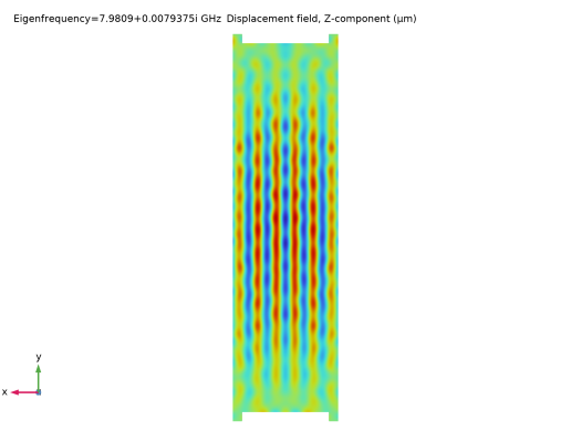
In the Model Builder window, under Frequency Domain - 7.95 to 8.05 GHz click Step 1: Frequency Domain.
2
In the Settings window for Frequency Domain, locate the Study Settings section.
3
From the Frequency unit list, choose GHz.
4
Click  Range.
5
In the Range dialog, type 7.95 in the Start text field.
6
In the Step text field, type 0.005.
7
In the Stop text field, type 8.05.
8
Click Add.
9
In the Study toolbar, click  Compute.
With the solution from Frequency Domain study, plot the admittance versus frequency and add a Graph Marker to return the coordinates of the maximum and minimum values.
Results
Admittance vs. Frequency (Frequency Domain)
1
In the Results toolbar, click  1D Plot Group.
2
In the Settings window for 1D Plot Group, type Admittance vs. Frequency (Frequency Domain) in the Label text field.
3
Locate the Data section. From the Dataset list, choose Frequency Domain - 7.95 to 8.05 GHz/Solution 2 (sol2).
4
Click to expand the Title section. From the Title type list, choose Manual.
5
In the Title text area, type Global: Admittance vs. Frequency.
6
Locate the Plot Settings section.
7
Select the y-axis label checkbox. In the associated text field, type log10(abs(Y11)).
8
Locate the Axis section. Select the Manual axis limits checkbox.
9
In the x minimum text field, type 7.92.
10
In the x maximum text field, type 8.08.
11
In the y minimum text field, type -4.7.
12
In the y maximum text field, type -3.0.
13
Locate the Legend section. Clear the Show legends checkbox.
Global 1
1
Right-click Admittance vs. Frequency (Frequency Domain) and choose Global.
2
In the Settings window for Global, locate the y-Axis Data section.
3
Graph Marker 1
1
Right-click Global 1 and choose Graph Marker.
2
In the Settings window for Graph Marker, locate the Text Format section.
3
Select the Show x-coordinate checkbox.
4
In the Admittance vs. Frequency (Frequency Domain) toolbar, click  Plot.
Result Templates
1
In the Results toolbar, click  Result Templates to open the Result Templates window.
2
Go to the Result Templates window.
3
In the tree, select Frequency Domain - 7.95 to 8.05 GHz/Solution 2 (sol2) > Layered Shell > Geometry and Layup (lshell) > Shell Geometry (lshell).
4
Click the Add Result Template button in the window toolbar.
5
In the Results toolbar, click  Result Templates to close the Result Templates window.
Results
Shell Geometry (lshell)
1
Click the  Zoom Extents button in the Graphics toolbar.
2
Click the  Show Grid button in the Graphics toolbar.
Stack Zones
1
In the Model Builder window, right-click Shell Geometry (lshell) and choose Duplicate.
2
In the Settings window for 3D Plot Group, type Stack Zones in the Label text field.
Surface 1
1
In the Model Builder window, expand the Stack Zones node, then click Surface 1.
2
In the Settings window for Surface, locate the Expression section.
3
In the Expression text field, type stlmat1.zone.
4
Locate the Coloring and Style section. From the Coloring list, choose Color table.
5
From the Color table list, choose TrafficLight.
Stack Zones
1
In the Model Builder window, click Stack Zones.
2
Drag and drop below Layer Cross-Section Preview.
3
In the Stack Zones toolbar, click  Plot.