PDF

Resonant Spiral Coil in 3D
Introduction
This application presents a self-resonating, 5-turn spiral coil of copper wire with 1 mm square cross section. The wire is equipped with a thin epoxy varnish insulation layer, tightly wound and mounted on a printed circuit board (PCB). It is fed by lines on the reverse side of the PCB. The capacitive coupling between the consecutive turns separated by the geometrically thin varnish layer is modeled using a special boundary condition in the Magnetic and Electric Fields interface, thereby avoiding costly volumetric meshing. In order to efficiently resolve the small skin depth in the copper a Boundary Layer mesh is used. The modeling of thin insulation layers and a small skin depth effectively becomes intractable in 3D if traditional volumetric meshing has to be employed for capturing such effects. As shown in the axisymmetric variant of this model, Resonant Spiral Coil in 2D Axisymmetry, it is a challenging task already in 2D.
The purpose of the application is to investigate the self-resonance of the coil. This is done by sweeping the frequency through the regime where the coil reactance transitions from inductive at frequencies below resonance to capacitive at frequencies above resonance.
Model Definition
The model geometry consists of the spiral-shaped copper inductor with feed lines, the printed circuit board (PCB), and the surrounding air. Figure 1 shows the inductor and PCB domains used in the model. The outer diameter of the coil is about 20 mm.
Figure 1: Spiral coil geometry including the PCB and feed lines on the back side.
The application uses the Magnetic and Electric Fields interface, taking electric and magnetically induced currents into account. This formulation, often referred to as an AV-formulation, solves both for the magnetic vector potential A and the electric potential V. The model is solved with a free gauge, using an iterative, residual minimizing method.
Using the definitions of the electric and magnetic potentials, the system of equations becomes
In the equations above, A denotes the magnetic vector potential, V the electric scalar potential, Je the externally generated or prescribed current density vector, σ the electric conductivity, ε0 the permittivity in vacuum, εr the relative permittivity, μ0 the permeability in vacuum, and μr the relative permeability. The first equation is the equation of continuity, stating the conservation of charge. The second equation is Maxwell–Ampère’s law. Because the model is excited using boundary constraints for the electric scalar potential, the externally generated current density, Je is zero everywhere.
The application uses the Terminal boundary condition, which applies an electric potential of 5 mV at the end of one feed line and the Ground boundary condition at the end of the other feed line. A Terminal feature defines one entry in the admittance matrix, here a scalar since there is only one Terminal. The feed impedance Z is defined as the reciprocal value of the single Y11 component of the admittance matrix.
Using an AV-formulation allows for an interior boundary condition representing a thin, insulating or highly resistive, dielectric layer, relating the normal component of the total (displacement + conduction) current density to a discontinuity in the electric potential while the magnetic vector potential and the magnetic flux density are continuous over the boundary. This Magnetic Continuity boundary condition with a Contact Impedance subfeature is applied on all boundaries exterior to the copper domains save the end feeds where the Terminal and Ground conditions are applied.
Results
Figure 2 shows the current density in the coil at the resonance frequency. The skin and proximity effects are pronounced with the current flow concentrated to the edges of the turns.
Figure 2: Current density in the coil exhibiting pronounced skin and proximity effects.
Figure 3 displays the feed impedance of the coil where the reactance transitions from inductive at frequencies below resonance to capacitive at frequencies above resonance.
Figure 3: The feed impedance (resistance and reactance) is shown. Note the transition from inductive (positive) to capacitive (negative) reactance at the resonance frequency.
Application Library path: ACDC_Module/Tutorials,_Coils/resonant_spiral_coil_3d
Modeling Instructions
From the File menu, choose New.
New
In the New window, click  Model Wizard.
Model Wizard
1
In the Model Wizard window, click  3D.
2
In the Select Physics tree, select AC/DC > Electromagnetic Fields > Vector Formulations > Magnetic and Electric Fields (mef).
3
Click Add.
4
Click  Study.
5
In the Select Study tree, select General Studies > Frequency Domain.
6
Define all the required parameters.
Global Definitions
Parameters 1
1
In the Model Builder window, under Global Definitions click Parameters 1.
2
In the Settings window for Parameters, locate the Parameters section.
3
Component 1 (comp1)
1
In the Model Builder window, click Component 1 (comp1).
2
In the Settings window for Component, locate the Curved Mesh Elements section.
3
From the Geometry shape function list, choose Linear Lagrange.
4
Clear the Avoid inverted elements by curving interior domain elements checkbox.
Geometry 1
Insert the geometry sequence from the resonant_spiral_coil_3d_geom_sequence.mph file.
1
In the Geometry toolbar, click Insert Sequence and choose Insert Sequence.
2
3
In the Geometry toolbar, click  Build All.
Disable the analysis of the geometry as the remaining small geometric details can be kept.
4
In the Model Builder window, click Geometry 1.
5
In the Settings window for Geometry, locate the Cleanup section.
6
Clear the Automatic detection of small details checkbox.
Definitions
Copper Surface
1
In the Model Builder window, expand the Component 1 (comp1) > Definitions node.
2
Right-click Definitions and choose Selections > Explicit.
3
In the Settings window for Explicit, type Copper Surface in the Label text field.
4
Locate the Input Entities section. Click  Paste Selection.
5
In the Paste Selection dialog, type 4-8 in the Selection text field.
6
7
In the Settings window for Explicit, locate the Output Entities section.
8
From the Output entities list, choose Adjacent boundaries.
Copper Domains
1
In the Definitions toolbar, click  Explicit.
2
In the Settings window for Explicit, type Copper Domains in the Label text field.
3
Locate the Input Entities section. Click  Paste Selection.
4
In the Paste Selection dialog, type 4-8 in the Selection text field.
5
Contact Boundaries
1
In the Definitions toolbar, click  Explicit.
2
In the Settings window for Explicit, type Contact Boundaries in the Label text field.
3
Locate the Input Entities section. From the Geometric entity level list, choose Boundary.
4
Click  Paste Selection.
5
In the Paste Selection dialog, type 32 in the Selection text field.
6
Copper and Contact Boundaries
1
In the Definitions toolbar, click  Union.
2
In the Settings window for Union, type Copper and Contact Boundaries in the Label text field.
3
Locate the Geometric Entity Level section. From the Level list, choose Boundary.
4
Locate the Input Entities section. Under Selections to add, click  Add.
5
In the Add dialog, select Contact Boundaries in the Selections to add list.
6
7
In the Settings window for Union, locate the Input Entities section.
8
Under Selections to add, click  Add.
9
In the Add dialog, select Copper Surface in the Selections to add list.
10
Copper Edges
1
In the Definitions toolbar, click  Explicit.
2
In the Settings window for Explicit, type Copper Edges in the Label text field.
3
Locate the Input Entities section. Click  Paste Selection.
4
In the Paste Selection dialog, type 4-8 in the Selection text field.
5
6
In the Settings window for Explicit, locate the Output Entities section.
7
From the Output entities list, choose Adjacent edges.
Feed and Ground
1
In the Definitions toolbar, click  Explicit.
2
In the Settings window for Explicit, type Feed and Ground in the Label text field.
3
Locate the Input Entities section. From the Geometric entity level list, choose Boundary.
4
Click  Paste Selection.
5
In the Paste Selection dialog, type 20, 43 in the Selection text field.
6
Varnish Boundaries
1
In the Definitions toolbar, click  Difference.
2
In the Settings window for Difference, type Varnish Boundaries in the Label text field.
3
Locate the Geometric Entity Level section. From the Level list, choose Boundary.
4
Locate the Input Entities section. Under Selections to add, click  Add.
5
In the Add dialog, select Copper and Contact Boundaries in the Selections to add list.
6
7
In the Settings window for Difference, locate the Input Entities section.
8
Under Selections to subtract, click  Add.
9
In the Add dialog, select Feed and Ground in the Selections to subtract list.
10
View 1
1
In the Model Builder window, under Component 1 (comp1) > Definitions click View 1.
2
In the Settings window for View, locate the View section.
3
Clear the Show grid checkbox.
Add Material
1
In the Materials toolbar, click  Add Material to open the Add Material window.
2
Go to the Add Material window.
3
In the tree, select Built-in > Copper.
4
Click the Add to Component button in the window toolbar.
Materials
Copper (mat1)
1
In the Settings window for Material, locate the Geometric Entity Selection section.
2
From the Selection list, choose Copper Domains.
Add Material
1
Go to the Add Material window.
2
In the tree, select AC/DC > FR4 (Circuit Board).
3
Click the Add to Component button in the window toolbar.
Materials
FR4 (Circuit Board) (mat2)
1
In the Settings window for Material, locate the Geometric Entity Selection section.
2
Click  Paste Selection.
3
In the Paste Selection dialog, type 2 in the Selection text field.
4
5
In the Settings window for Material, locate the Material Contents section.
6
Add Material
1
Go to the Add Material window.
2
Click the Add to Component button in the window toolbar.
3
In the Materials toolbar, click  Add Material to close the Add Material window.
Materials
FR4 (Circuit Board) 1 (mat3)
1
In the Settings window for Material, locate the Geometric Entity Selection section.
2
From the Geometric entity level list, choose Boundary.
3
From the Selection list, choose Varnish Boundaries.
4
Locate the Material Contents section. In the table, enter the following settings:
Magnetic and Electric Fields (mef)
1
In the Model Builder window, under Component 1 (comp1) click Magnetic and Electric Fields (mef).
2
In the Settings window for Magnetic and Electric Fields, click to expand the Discretization section.
3
From the Magnetic vector potential list, choose Linear.
4
From the Electric potential list, choose Linear.
Magnetic Insulation 1
In the Model Builder window, under Component 1 (comp1) > Magnetic and Electric Fields (mef) click Magnetic Insulation 1.
Electric Insulation 1
1
In the Physics toolbar, click  Attributes and choose Electric Insulation.
2
In the Settings window for Electric Insulation, locate the Boundary Selection section.
3
From the Selection list, choose All boundaries.
Magnetic Insulation 1
In the Model Builder window, click Magnetic Insulation 1.
Boundary Terminal 1
1
In the Physics toolbar, click  Attributes and choose Boundary Terminal.
2
In the Settings window for Boundary Terminal, locate the Boundary Selection section.
3
Click  Paste Selection.
4
In the Paste Selection dialog, type 20 in the Selection text field.
5
6
In the Settings window for Boundary Terminal, locate the Terminal section.
7
From the Terminal type list, choose Voltage.
8
In the V0 text field, type 5[mV].
Magnetic Insulation 1
In the Model Builder window, click Magnetic Insulation 1.
Ground 2
1
In the Physics toolbar, click  Attributes and choose Ground.
2
In the Settings window for Ground, locate the Boundary Selection section.
3
Click  Paste Selection.
4
In the Paste Selection dialog, type 43 in the Selection text field.
5
Ampère’s Law and Current Conservation in Solids 1
1
In the Physics toolbar, click  Domains and choose Ampère’s Law and Current Conservation in Solids.
2
Magnetic Continuity 1
1
In the Physics toolbar, click  Boundaries and choose Magnetic Continuity.
2
In the Settings window for Magnetic Continuity, locate the Boundary Selection section.
3
From the Selection list, choose Varnish Boundaries.
Contact Impedance 1
1
In the Physics toolbar, click  Attributes and choose Contact Impedance.
2
In the Settings window for Contact Impedance, locate the Boundary Selection section.
3
From the Selection list, choose Varnish Boundaries.
4
Locate the Contact Impedance section. In the ds text field, type 0.0001[mm].
Magnetic Continuity 1
In the Model Builder window, click Magnetic Continuity 1.
Contact Impedance 2
1
In the Physics toolbar, click  Attributes and choose Contact Impedance.
2
In the Settings window for Contact Impedance, locate the Boundary Selection section.
3
From the Selection list, choose Contact Boundaries.
4
Locate the Contact Impedance section. In the ds text field, type 0.0002[mm].
Note that two different Contact Impedance subfeatures are added to the Magnetic Continuity feature, since the varnish layer is twice as thick on the inner boundaries where the coil is in contact with itself.
Mesh 1
1
In the Model Builder window, under Component 1 (comp1) click Mesh 1.
2
In the Settings window for Mesh, locate the Sequence Type section.
3
From the list, choose User-controlled mesh.
Size 1
1
Right-click Component 1 (comp1) > Mesh 1 and choose Size.
2
Drag and drop Size 1 below Size.
3
In the Settings window for Size, locate the Geometric Entity Selection section.
4
From the Geometric entity level list, choose Edge.
5
From the Selection list, choose Copper Edges.
6
Locate the Element Size section. Click the Custom button.
7
Locate the Element Size Parameters section.
8
Select the Maximum element size checkbox. In the associated text field, type 0.2.
9
Click  Build Selected.
Size 2
1
In the Model Builder window, right-click Mesh 1 and choose Size.
2
In the Settings window for Size, locate the Geometric Entity Selection section.
3
From the Geometric entity level list, choose Domain.
4
From the Selection list, choose Copper Domains.
5
Locate the Element Size section. Click the Custom button.
6
Locate the Element Size Parameters section.
7
Select the Maximum element size checkbox. In the associated text field, type 0.5.
8
Click  Build Selected.
Now, add a Boundary Layer mesh. This is needed in order to resolve the small skin depth in the varnish layer without making the model too computationally heavy.
Boundary Layers 1
1
In the Mesh toolbar, click  Boundary Layers.
2
In the Settings window for Boundary Layers, locate the Geometric Entity Selection section.
3
From the Geometric entity level list, choose Domain.
4
From the Selection list, choose Copper Domains.
Boundary Layer Properties
1
In the Model Builder window, click Boundary Layer Properties.
2
In the Settings window for Boundary Layer Properties, locate the Boundary Selection section.
3
From the Selection list, choose Copper and Contact Boundaries.
4
Locate the Layers section. In the Number of layers text field, type 4.
5
In the Stretching factor text field, type 1.5.
6
From the Thickness specification list, choose First layer.
7
In the Thickness text field, type delta/2.
8
Click  Build Selected.
Free Tetrahedral 1
1
In the Model Builder window, under Component 1 (comp1) > Mesh 1 click Free Tetrahedral 1.
2
In the Settings window for Free Tetrahedral, click to expand the Element Quality Optimization section.
3
Click  Build Selected.
4
In the Mesh toolbar, click  Plot.
Results
Mesh Plot
1
In the Model Builder window, under Results click Mesh Plot 1.
2
In the Settings window for 3D Plot Group, type Mesh Plot in the Label text field.
Mesh 1
1
In the Model Builder window, click Mesh 1.
2
In the Settings window for Mesh, locate the Coloring and Style section.
3
From the Color table list, choose TrafficLightClassic.
4
From the Color table transformation list, choose Reverse.
5
Click to expand the Element Filter section. Select the Enable filter checkbox.
6
In the Expression text field, type y>1[mm].
Selection 1
1
Right-click Mesh 1 and choose Selection.
2
In the Settings window for Selection, locate the Selection section.
3
From the Selection list, choose Copper Domains.
Mesh Plot
1
In the Model Builder window, under Results click Mesh Plot.
2
In the Mesh Plot toolbar, click  Plot.
3
Click the  Go to Default View button in the Graphics toolbar.
The plot shows the Mesh.
The last step consists of setting up the study. Since the electric potential converges rather slowly, the stationary tolerance needs to be tightened a bit in order to get accurate results. Then, set up an iterative solver.
Study 1
1
In the Model Builder window, click Study 1.
2
In the Settings window for Study, locate the Study Settings section.
3
Clear the Generate default plots checkbox.
Step 1: Frequency Domain
1
In the Model Builder window, under Study 1 click Step 1: Frequency Domain.
2
In the Settings window for Frequency Domain, locate the Study Settings section.
3
In the Frequencies text field, type range(5600000,28000,7000000).
When studying frequencies near resonance with the Magnetic and Electrical Fields interface, it can be advantageous to decrease the solver tolerance to enable the solver to converge on the correct solution. In this case, a very tight tolerance of 1e-9 is needed.
4
From the Reuse solution from previous step list, choose Auto.
5
From the Tolerance list, choose User controlled.
6
In the Relative tolerance text field, type 1e-9.
The special boundary conditions used in this model to represent the thin varnish layers require some further adjustments to the default solver settings. Namely, implementing a direct preconditioner for the discontinuous V.
Solution 1 (sol1)
1
In the Study toolbar, click  Show Default Solver.
2
In the Model Builder window, expand the Solution 1 (sol1) node.
3
In the Model Builder window, expand the Study 1 > Solver Configurations > Solution 1 (sol1) > Stationary Solver 1 node, then click Iterative 1.
4
In the Settings window for Iterative, locate the General section.
5
From the Solver list, choose BiCGStab.
6
From the Preconditioning list, choose Right.
7
Click to expand the Error section. In the Factor in error estimate text field, type 400.
8
Right-click Study 1 > Solver Configurations > Solution 1 (sol1) > Stationary Solver 1 > Iterative 1 and choose Direct Preconditioner.
9
In the Settings window for Direct Preconditioner, locate the General section.
10
From the Solver list, choose PARDISO.
11
Click to expand the Hybridization section. From the Use as list, choose Multi preconditioner.
12
In the Preconditioner variables list box, select Magnetic Vector Potential (comp1.A).
13
Under Preconditioner variables, click  Delete.
14
Right-click Iterative 1 and choose SOR.
15
In the Settings window for SOR, locate the General section.
16
In the Number of iterations text field, type 3.
17
Click to expand the Hybridization section. In the Preconditioner variables list box, select Electric Potential (comp1.V).
18
Under Preconditioner variables, click  Delete.
Definitions
Global Variable Probe 1 (var1)
1
In the Definitions toolbar, click  Probes and choose Global Variable Probe.
2
In the Settings window for Global Variable Probe, locate the Expression section.
3
In the Expression text field, type real(1/mef.Y11).
Global Variable Probe 2 (var2)
1
In the Definitions toolbar, click  Probes and choose Global Variable Probe.
2
In the Settings window for Global Variable Probe, locate the Expression section.
3
In the Expression text field, type imag(1/mef.Y11).
Study 1
In the Study toolbar, click  Compute.
Results
B, J and V
1
In the Results toolbar, click  3D Plot Group.
2
In the Settings window for 3D Plot Group, type B, J and V in the Label text field.
3
Locate the Data section. From the Parameter value (freq (Hz)) list, choose 6.188E6.
4
Locate the Plot Settings section. Clear the Plot dataset edges checkbox.
Slice 1
1
Right-click B, J and V and choose Slice.
2
In the Settings window for Slice, locate the Expression section.
3
In the Expression text field, type log(mef.normJ).
4
Locate the Plane Data section. From the Plane list, choose zx-planes.
5
From the Entry method list, choose Coordinates.
6
In the y-coordinates text field, type -2.
7
Locate the Coloring and Style section. From the Color table list, choose Prism.
Selection 1
1
Right-click Slice 1 and choose Selection.
2
In the Settings window for Selection, locate the Selection section.
3
Click  Paste Selection.
4
In the Paste Selection dialog, type 4 in the Selection text field.
5
Arrow Surface 1
1
In the Model Builder window, right-click B, J and V and choose Arrow Surface.
2
In the Settings window for Arrow Surface, locate the Expression section.
3
In the x-component text field, type side(4,mef.Jx).
4
In the y-component text field, type side(4,mef.Jy).
5
In the z-component text field, type side(4,mef.Jz).
6
Locate the Arrow Positioning section. From the Placement list, choose Gauss points.
7
Locate the Coloring and Style section. From the Arrow type list, choose Cone.
8
From the Arrow length list, choose Logarithmic.
9
In the Range quotient text field, type 25.
10
From the Arrow base list, choose Center.
Selection 1
1
Right-click Arrow Surface 1 and choose Selection.
2
In the Settings window for Selection, locate the Selection section.
3
From the Selection list, choose Copper Surface.
Color Expression 1
1
In the Model Builder window, right-click Arrow Surface 1 and choose Color Expression.
2
In the Settings window for Color Expression, locate the Coloring and Style section.
3
Clear the Color legend checkbox.
4
Locate the Expression section. In the Expression text field, type mef.normJ.
5
In the Unit field, type A/mm^2.
6
Locate the Coloring and Style section. From the Color table list, choose GrayScale.
Line 1
1
In the Model Builder window, right-click B, J and V and choose Line.
2
In the Settings window for Line, locate the Expression section.
3
In the Expression text field, type 1.
4
Locate the Coloring and Style section. From the Coloring list, choose Uniform.
5
From the Color list, choose Gray.
Selection 1
1
Right-click Line 1 and choose Selection.
2
In the Settings window for Selection, locate the Selection section.
3
From the Selection list, choose Copper Edges.
Volume 1
1
In the Model Builder window, right-click B, J and V and choose Volume.
2
In the Settings window for Volume, locate the Coloring and Style section.
3
From the Color table list, choose Dipole.
Selection 1
1
Right-click Volume 1 and choose Selection.
2
In the Settings window for Selection, locate the Selection section.
3
Click  Paste Selection.
4
In the Paste Selection dialog, type 2 in the Selection text field.
5
Transparency 1
1
In the Model Builder window, right-click Volume 1 and choose Transparency.
2
In the Settings window for Transparency, locate the Transparency section.
3
Find the Fresnel transmittance subsection. In the Fresnel transmittance text field, type 0.5.
Arrow Volume 1
1
In the Model Builder window, right-click B, J and V and choose Arrow Volume.
2
In the Settings window for Arrow Volume, locate the Arrow Positioning section.
3
Find the x grid points subsection. In the Points text field, type 40.
4
Find the y grid points subsection. In the Points text field, type 1.
5
Find the z grid points subsection. In the Points text field, type 40.
6
Locate the Coloring and Style section. From the Arrow length list, choose Logarithmic.
7
From the Arrow base list, choose Center.
Color Expression 1
1
Right-click Arrow Volume 1 and choose Color Expression.
2
In the Settings window for Color Expression, locate the Expression section.
3
In the Expression text field, type mef.normB.
4
Locate the Coloring and Style section. From the Color table list, choose PrismDark.
5
Clear the Color legend checkbox.
B, J and V
1
In the Model Builder window, under Results click B, J and V.
2
In the B, J and V toolbar, click  Plot.
3
Click the  Scene Light button in the Graphics toolbar.
4
Click the  Go to Default View button in the Graphics toolbar.
The Arrow Volume shows the Magnetic flux density. The volume shows the Electric potential. The Arrow Surface shows the Current density.
Normal (displacement) current density
1
In the Results toolbar, click  3D Plot Group.
2
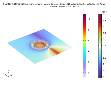
In the Settings window for 3D Plot Group, type Normal (displacement) current density in the Label text field.
3
Locate the Data section. From the Parameter value (freq (Hz)) list, choose 6.188E6.
4
Locate the Plot Settings section. Clear the Plot dataset edges checkbox.
Surface 1
1
Right-click Normal (displacement) current density and choose Surface.
2
In the Settings window for Surface, locate the Expression section.
3
In the Expression text field, type abs(mef.mc1.ci2.nJ).
4
In the Unit field, type A/mm^2.
5
Locate the Coloring and Style section. From the Color table list, choose RainbowLightClassic.
Selection 1
1
Right-click Surface 1 and choose Selection.
2
In the Settings window for Selection, locate the Selection section.
3
From the Selection list, choose Contact Boundaries.
Line 1
1
In the Model Builder window, right-click Normal (displacement) current density and choose Line.
2
In the Settings window for Line, locate the Expression section.
3
In the Expression text field, type 1.
4
Locate the Coloring and Style section. From the Coloring list, choose Uniform.
5
From the Color list, choose Gray.
Selection 1
1
Right-click Line 1 and choose Selection.
2
In the Settings window for Selection, locate the Selection section.
3
From the Selection list, choose Copper Edges.
Normal (displacement) current density
1
In the Model Builder window, under Results click Normal (displacement) current density.
2
In the Normal (displacement) current density toolbar, click  Plot.
3
Click the  Go to Default View button in the Graphics toolbar.
The plot shows the Normal current density.
|J|
1
In the Results toolbar, click  3D Plot Group.
2
In the Settings window for 3D Plot Group, type |J| in the Label text field.
3
Locate the Data section. From the Parameter value (freq (Hz)) list, choose 6.188E6.
4
Locate the Plot Settings section. Clear the Plot dataset edges checkbox.
Line 1
1
Right-click |J| and choose Line.
2
In the Settings window for Line, locate the Expression section.
3
In the Expression text field, type 1.
4
Locate the Coloring and Style section. From the Coloring list, choose Uniform.
5
From the Color list, choose Gray.
Selection 1
1
Right-click Line 1 and choose Selection.
2
In the Settings window for Selection, locate the Selection section.
3
From the Selection list, choose Copper Edges.
Volume 1
1
In the Model Builder window, right-click |J| and choose Volume.
2
In the Settings window for Volume, locate the Expression section.
3
In the Expression text field, type mef.normJ.
4
In the Unit field, type A/mm^2.
5
Locate the Coloring and Style section. From the Color table list, choose HeatCameraLight.
6
From the Color table transformation list, choose Reverse.
7
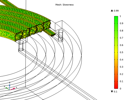
Click to expand the Quality section.
Selection 1
1
Right-click Volume 1 and choose Selection.
2
In the Settings window for Selection, locate the Selection section.
3
From the Selection list, choose Copper Domains.
|J|
1
In the Model Builder window, under Results click |J|.
2
In the |J| toolbar, click  Plot.
3
Click the  Go to Default View button in the Graphics toolbar.
The Volume plot shows the norm of the current density.
Feed Impedance
1
In the Results toolbar, click  1D Plot Group.
2
In the Settings window for 1D Plot Group, type Feed Impedance in the Label text field.
Global 1
1
Right-click Feed Impedance and choose Global.
2
In the Settings window for Global, locate the y-Axis Data section.
3
4
Click to expand the Coloring and Style section. From the Width list, choose 3.
Feed Impedance
1
In the Model Builder window, click Feed Impedance.
2
In the Feed Impedance toolbar, click  Plot.