| 
|
|
|
|

|
1
|
|
2
|
Browse to the model’s Application Libraries folder and double-click the file igbt_joule_heating_introduction.mph.
|
|
3
|
|
4
|
Browse to a suitable folder and type the filename igbt_joule_heating.mph.
|
|
1
|
|
2
|
Go to the Add Physics window.
|
|
3
|
|
4
|
Click the Add to Component 1 button in the window toolbar.
|
|
1
|
|
2
|
|
3
|
|
1
|
|
2
|
|
3
|
|
1
|
|
2
|
|
3
|
|
4
|
|
1
|
|
2
|
|
3
|
|
4
|
|
1
|
Go to the Add Physics window.
|
|
2
|
|
3
|
Click the Add to Component 1 button in the window toolbar.
|
|
1
|
|
2
|
|
3
|
|
1
|
In the Model Builder window, under Component 1 (comp1) > Heat Transfer in Solids (ht) click Initial Values 1.
|
|
2
|
|
3
|
|
1
|
|
2
|
|
3
|
|
4
|
|
1
|
|
2
|
|
3
|
|
4
|
|
5
|
|
6
|
|
1
|
|
2
|
|
3
|
|
4
|
Locate the Shell Properties section. From the Shell type list, choose Nonlayered shell. In the Lth text field, type th_met.
|
|
5
|
|
1
|
|
2
|
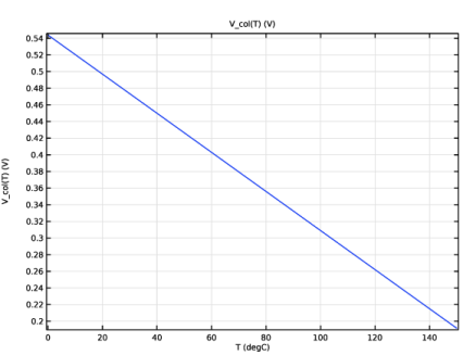
In the Settings window for Analytic, type Collector-Emitter Voltage IGBT (Open) in the Label text field.
|
|
3
|
|
4
|
|
5
|
|
6
|
|
8
|
Locate the Plot Parameters section. In the table, enter the following settings:
|
|
9
|
|
1
|
|
2
|
|
3
|
|
4
|
|
1
|
Go to the Add Physics window.
|
|
2
|
|
3
|
Click the Add to Component 1 button in the window toolbar.
|
|
4
|
|
1
|
|
2
|
Locate the Global Equations section. In the table, enter the following settings:
|
|
3
|
|
4
|
|
5
|
Click OK.
|
|
6
|
|
7
|
Click
|
|
8
|
|
9
|
Click OK.
|
|
1
|
|
2
|
|
3
|
Locate the Global Equations section. In the table, enter the following settings:
|
|
4
|
|
5
|
|
6
|
Click OK.
|
|
7
|
|
8
|
Click
|
|
9
|
|
10
|
Click OK.
|
|
1
|
|
2
|
|
3
|
Locate the Variables section. In the table, enter the following settings:
|
|
1
|
In the Model Builder window, under Component 1 (comp1) > Materials, add the following material properties:
|
|
1
|
|
2
|
|
1
|
|
2
|
Go to the Add Study window.
|
|
3
|
|
4
|
Click the Add Study button in the window toolbar.
|
|
5
|
|
1
|
|
2
|
|
3
|
In the Model Builder window, expand the Study 1 > Solver Configurations > Solution 1 (sol1) > Stationary Solver 1 > Segregated 1 node, then click Electric Currents.
|
|
4
|
|
5
|
|
6
|
In the Model Builder window, under Study 1 > Solver Configurations > Solution 1 (sol1) > Stationary Solver 1 > Segregated 1 click Temperature.
|
|
7
|
|
8
|
|
9
|
Right-click Study 1 > Solver Configurations > Solution 1 (sol1) > Stationary Solver 1 > Segregated 1 > Temperature and choose Move Up.
|
|
10
|
Right-click Study 1 > Solver Configurations > Solution 1 (sol1) > Stationary Solver 1 > Segregated 1 > Lower Limit 1 and choose Move Up.
|
|
11
|
|
12
|
|
13
|
Clear the Generate default plots checkbox.
|
|
14
|
|
1
|
|
2
|
|
3
|
Select the Only plot when requested checkbox, since the resulting plots will take a while to evaluate.
|
|
4
|
|
1
|
|
2
|
|
1
|
|
2
|
|
3
|
|
4
|
|
1
|
|
2
|
|
3
|
|
4
|
|
1
|
|
2
|
|
3
|
|
4
|
|
5
|
|
1
|
|
2
|
|
3
|
|
4
|
|
5
|
|
1
|
|
2
|
|
3
|
|
4
|
|
5
|
|
6
|
|
7
|
|
1
|
|
2
|
|
3
|
|
4
|
|
5
|
|
6
|
|
7
|
Click OK.
|
|
1
|
|
2
|
|
3
|
|
4
|
|
1
|
|
2
|
|
3
|
|
4
|
|
5
|
|
1
|
|
2
|
|
3
|
|
4
|
|
5
|
|
1
|
|
2
|
|
3
|
|
4
|
|
5
|
|
6
|
|
7
|
|
1
|
|
2
|
|
3
|
|
1
|
|
2
|
|
3
|
|
4
|
|
5
|
|
6
|
|
1
|
|
2
|
|
3
|
|
1
|
|
2
|
|
3
|
|
4
|
|
5
|
|
6
|
|
7
|
|
1
|
|
2
|
|
3
|
|
1
|
|
2
|
|
3
|
|
4
|
|
5
|
|
1
|
|
2
|
|
3
|
|
4
|
|
5
|
|
1
|
|
2
|
|
3
|
|
4
|
|
5
|
|
6
|
|
7
|
|
8
|
|
1
|
|
2
|
|
3
|
|
4
|
|
5
|
|
6
|
|
7
|
|
1
|
|
2
|
|
3
|
|
1
|
|
2
|
|
3
|
|
4
|
|
5
|
|
1
|
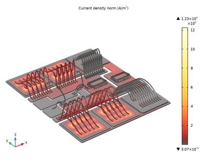
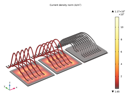
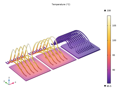
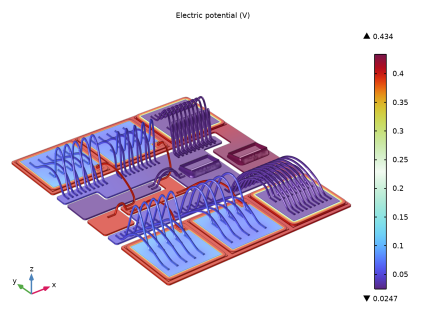
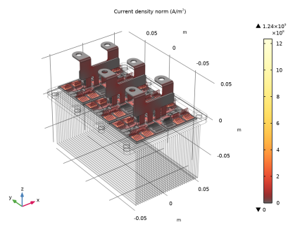
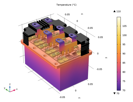
In the Model Builder window, under Results, Ctrl-click to select Electric Potential (ec), Current Density Norm (ec), and Temperature (ht).
|
|
2
|
Right-click and choose Group.
|
|
1
|
|
2
|
|
3
|
|
1
|
|
2
|
|
3
|
|
4
|
|
1
|
|
2
|
|
3
|
|
4
|
|
1
|
|
2
|
|
3
|
|
4
|
|
5
|
|
1
|
|
2
|
|
3
|
|
4
|
|
1
|
In the Model Builder window, expand the Results > Module Section > Current Density Norm (ec) 1 > Surface 1 node, then click Selection 1.
|
|
2
|
|
3
|
|
1
|
In the Model Builder window, expand the Results > Module Section > Current Density Norm (ec) 1 > Surface 2 node, then click Selection 1.
|
|
2
|
|
3
|
|
1
|
|
2
|
|
3
|
|
4
|
|
5
|
|
1
|
|
2
|
|
3
|
|
4
|
|
5
|
|
6
|
|
1
|
|
2
|
|
1
|
|
2
|
|
3
|
|
1
|
|
2
|
|
3
|
|
4
|
|
5
|
|
1
|
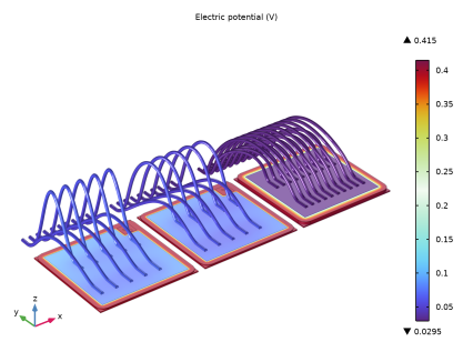
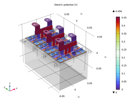
In the Model Builder window, expand the Results > All Domains > Electric Potential (ec) 2 > Line 1 node.
|
|
2
|
|
3
|
|
4
|
|
5
|
|
1
|
|
2
|
|
3
|
|
4
|
|
5
|
|
1
|
|
2
|
|
3
|
|
4
|
|
1
|
In the Model Builder window, expand the Results > All Domains > Current Density Norm (ec) 2 > Surface 1 node, then click Selection 1.
|
|
2
|
|
3
|
|
1
|
In the Model Builder window, expand the Results > All Domains > Current Density Norm (ec) 2 > Surface 2 node, then click Selection 1.
|
|
2
|
|
3
|
|
1
|
In the Model Builder window, expand the Results > All Domains > Current Density Norm (ec) 2 > Line 1 node.
|
|
2
|
|
3
|
|
4
|
|
5
|
|
1
|
|
2
|
|
3
|
|
4
|
|
5
|
|
1
|
|
2
|
|
3
|
|
1
|
|
2
|
|
3
|
|
4
|
|
5
|
|
1
|
|
2
|
|
3
|
|
4
|
|
1
|
|
2
|
|
3
|
|
1
|
|
2
|
|
3
|
|
1
|
|
2
|
|
3
|
|
4
|
|
1
|
|
2
|
|
3
|
|
1
|
|
2
|
|
3
|
|
4
|
|
5
|
|
1
|
|
2
|
|
3
|
|
4
|
|
5
|
|
1
|
|
2
|
|
1
|
|
2
|
|
3
|
Select the Transpose checkbox.
|
|
4
|
|
1
|
|
2
|
Click
|
|
1
|
|
2
|
|
1
|
|
2
|
|
3
|
Clear the Automatic detection of small details checkbox.
|
|
4
|
|
5
|
Select the Design Module Boolean operations checkbox.
|
|
1
|
|
2
|
|
3
|
|
4
|
Click
|
|
5
|
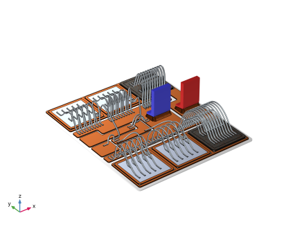
Browse to the model’s Application Libraries folder and double-click the file igbt_joule_heating_geom.step.
|
|
6
|
Click
|
|
7
|
|
8
|
|
10
|
|
12
|
|
13
|
|
1
|
|
2
|
|
3
|
|
4
|
|
5
|
Locate the Distances section. In the table, enter the following settings:
|
|
6
|
Select the Reverse direction checkbox.
|
|
7
|
Locate the Selections of Resulting Entities section. Select the Resulting objects selection checkbox.
|
|
8
|
Locate the Selections on Input Objects section. Clear the Propagate selections to resulting objects checkbox.
|
|
1
|
|
2
|
|
3
|
|
4
|
|
5
|
In the Add dialog, in the Selections to add list, choose IGBT Upper Electrode (Import 1) and Remaining Electrodes (Import 1).
|
|
6
|
Click OK.
|
|
1
|
|
2
|
|
3
|
|
4
|
In the Add dialog, in the Selections to add list, choose DCB Bottom Cu Layer (Import 1), DCB Upper Cu Layer (Import 1), Collector Busbar (Import 1), Emitter Busbar (Import 1), and Backing Plate (Import 1).
|
|
5
|
Click OK.
|
|
1
|
|
2
|
|
3
|
|
4
|
In the Add dialog, in the Selections to add list, choose DCB Solder (Import 1), Diode Solder (Import 1), IGBT Solder (Import 1), and Busbar Solder (Import 1).
|
|
5
|
Click OK.
|
|
1
|
|
2
|
|
3
|
|
4
|
In the Add dialog, in the Selections to add list, choose Bond Wires (Import 1) and Heat Sink (Import 1).
|
|
5
|
Click OK.
|
|
1
|
In the Model Builder window, under Component 1 (comp1) > Geometry 1, ctrl-click to select all nodes from Aluminum (Metalization) (unisel1) to Aluminum (unisel4).
|
|
2
|
Right-click and choose Group.
|
|
1
|
|
2
|
|
3
|
|
1
|
|
2
|
|
3
|
|
4
|
In the Add dialog, in the Selections to add list, choose IGBT Die (Import 1), Diode Die (Import 1), Bond Wires (Import 1), DCB Upper Cu Layer (Import 1), Collector Busbar (Import 1), Emitter Busbar (Import 1), Diode Solder (Import 1), IGBT Solder (Import 1), and Busbar Solder (Import 1).
|
|
5
|
Click OK.
|
|
1
|
|
2
|
In the Settings window for Complement Selection, type Heat Transfer Domains in the Label text field.
|
|
3
|
|
4
|
|
5
|
Click OK.
|
|
1
|
|
2
|
|
3
|
|
4
|
|
5
|
|
6
|
Click OK.
|
|
1
|
In the Model Builder window, under Component 1 (comp1) > Geometry 1, ctrl-click to select all nodes from Electric Current Domains (unisel5) to Fixed Temperature (unisel6).
|
|
2
|
Right-click and choose Group.
|
|
1
|
|
2
|
|
3
|
|
1
|
|
2
|
|
3
|
|
4
|
In the Add dialog, in the Selections to add list, choose DCB Bottom Cu Layer (Import 1), DCB Aluminum Oxide Layer (Import 1), and DCB Solder (Import 1).
|
|
5
|
Click OK.
|
|
1
|
|
2
|
|
3
|
|
4
|
In the Add dialog, in the Selections to add list, choose Collector Busbar (Import 1) and Emitter Busbar (Import 1).
|
|
5
|
Click OK.
|
|
1
|
|
2
|
|
3
|
|
4
|
In the Add dialog, in the Selections to add list, choose Diode Solder (Import 1) and IGBT Solder (Import 1).
|
|
5
|
Click OK.
|
|
1
|
|
2
|
|
3
|
|
4
|
In the Add dialog, in the Selections to add list, choose IGBT Die (Import 1) and Diode Die (Import 1).
|
|
5
|
Click OK.
|
|
1
|
|
2
|
In the Settings window for Union Selection, type IGBT and Diode Die and Solder in the Label text field.
|
|
3
|
|
4
|
In the Add dialog, in the Selections to add list, choose IGBT and Diode Solder and IGBT and Diode Die.
|
|
5
|
Click OK.
|
|
1
|
|
2
|
|
3
|
|
4
|
In the Add dialog, in the Selections to add list, choose DCB Upper Cu Layer (Import 1), Busbar Solder (Import 1), and Busbars.
|
|
5
|
Click OK.
|
|
1
|
|
2
|
|
3
|
|
4
|
In the Add dialog, in the Selections to add list, choose Thermal Paste (Import 1) and DCB Base Layers.
|
|
5
|
Click OK.
|
|
1
|
|
2
|
|
3
|
|
4
|
Click
|
|
5
|
|
6
|
Click OK.
|
|
7
|
|
8
|
|
1
|
|
2
|
|
3
|
|
4
|
Click
|
|
5
|
|
6
|
Click OK.
|
|
7
|
|
8
|
|
1
|
|
2
|
|
3
|
Click
|
|
4
|
|
5
|
Click OK.
|
|
6
|
|
7
|
|
1
|
|
2
|
In the Settings window for Logical Expression Selection, type Free Triangular 1 in the Label text field.
|
|
3
|
|
4
|
Locate the Expression section. In the Logical expression text area, type adjsel1 || (adjsel2 && adjsel3 && !imp1_Color_4).
|
|
5
|
|
1
|
|
2
|
|
3
|
|
4
|
|
5
|
|
6
|
Click OK.
|
|
7
|
|
8
|
|
9
|
|
10
|
Click OK.
|
|
1
|
|
2
|
In the Settings window for Adjacent Selection, type Boundary Layer Properties in the Label text field.
|
|
3
|
|
4
|
Click
|
|
5
|
|
6
|
Click OK.
|
|
7
|
|
8
|
|
9
|
|
10
|
Select the Interior edges checkbox.
|
|
1
|
|
2
|
|
3
|
|
4
|
|
5
|
|
6
|
|
7
|
|
8
|
|
9
|
|
10
|
Locate the Output Entities section. From the Include entity if list, choose All vertices inside box.
|
|
1
|
In the Model Builder window, under Component 1 (comp1) > Geometry 1, ctrl-click to select all nodes from DCB Base Layers (unisel7) to Free Tetrahedral 6: Size 2 (boxsel1).
|
|
2
|
Right-click and choose Group.
|
|
1
|
|
2
|
|
3
|
|
1
|
|
2
|
|
3
|
|
4
|
|
5
|
|
6
|
|
7
|
|
8
|
|
9
|
Locate the Output Entities section. From the Include entity if list, choose All vertices inside box.
|
|
1
|
|
2
|
|
3
|
|
4
|
|
5
|
Click OK.
|
|
6
|
|
7
|
Select the Interior boundaries checkbox.
|
|
1
|
|
2
|
In the Settings window for Difference Selection, type Set of Dies (Not Metalization) in the Label text field.
|
|
3
|
|
4
|
|
5
|
|
6
|
Click OK.
|
|
7
|
|
8
|
|
9
|
|
10
|
Click OK.
|
|
1
|
|
2
|
In the Settings window for Intersection Selection, type Set of Dies (Metalization) in the Label text field.
|
|
3
|
|
4
|
|
5
|
In the Add dialog, in the Selections to intersect list, choose Aluminum (Metalization) and Set of Dies (Boundary).
|
|
6
|
Click OK.
|
|
1
|
|
2
|
|
3
|
|
4
|
|
5
|
|
6
|
|
7
|
|
8
|
|
9
|
Locate the Output Entities section. From the Include entity if list, choose All vertices inside box.
|
|
1
|
|
2
|
In the Settings window for Adjacent Selection, type Module Section (Boundary) in the Label text field.
|
|
3
|
|
4
|
|
5
|
Click OK.
|
|
6
|
|
7
|
Select the Interior boundaries checkbox.
|
|
1
|
|
2
|
In the Settings window for Difference Selection, type Module Section (Not Metalization) in the Label text field.
|
|
3
|
|
4
|
|
5
|
|
6
|
Click OK.
|
|
7
|
|
8
|
|
9
|
|
10
|
Click OK.
|
|
1
|
|
2
|
In the Settings window for Intersection Selection, type Module Section (Metalization) in the Label text field.
|
|
3
|
|
4
|
|
5
|
In the Add dialog, in the Selections to intersect list, choose Aluminum (Metalization) and Module Section (Boundary).
|
|
6
|
Click OK.
|
|
1
|
|
2
|
|
3
|
|
4
|
|
5
|
Click OK.
|
|
6
|
|
7
|
|
8
|
|
9
|
Click OK.
|
|
1
|
|
2
|
In the Settings window for Adjacent Selection, type All Domains (EC, Boundary) in the Label text field.
|
|
3
|
|
4
|
|
5
|
Click OK.
|
|
1
|
|
2
|
In the Settings window for Difference Selection, type All Domains (EC, Not Metalization) in the Label text field.
|
|
3
|
|
4
|
|
5
|
|
6
|
Click OK.
|
|
7
|
|
8
|
|
9
|
|
10
|
Click OK.
|
|
1
|
|
2
|
In the Settings window for Intersection Selection, type All Domains (EC, Metalization) in the Label text field.
|
|
3
|
|
4
|
|
5
|
In the Add dialog, in the Selections to intersect list, choose Aluminum (Metalization) and All Domains (EC, Boundary).
|
|
6
|
Click OK.
|
|
1
|
In the Model Builder window, under Component 1 (comp1) > Geometry 1, ctrl-click to select all nodes from Set of Dies (Domain) (boxsel2) to All Domains (EC, Metalization) (intsel3).
|
|
2
|
Right-click and choose Group.
|
|
1
|
|
2
|
|
1
|
In the Model Builder window, collapse the Component 1 (comp1) > Geometry 1 > Results Selections node.
|
|
1
|
|
2
|
|
3
|
|
4
|
|
5
|
|
6
|
Clear the Short edges checkbox.
|
|
7
|
Clear the Small faces checkbox.
|
|
8
|
Clear the Sliver faces checkbox.
|
|
9
|
Clear the Thin domains checkbox.
|
|
10
|
|
11
|
|
12
|
Click
|
|
1
|
|
2
|
|
3
|
|
4
|
|
1
|
In the Model Builder window, under Component 1 (comp1) right-click Materials and choose Blank Material.
|
|
2
|
|
3
|
|
1
|
|
2
|
|
3
|
|
1
|
|
2
|
|
3
|
Locate the Geometric Entity Selection section. From the Geometric entity level list, choose Boundary.
|
|
4
|
|
1
|
|
2
|
|
3
|
Locate the Geometric Entity Selection section. From the Selection list, choose Diode Die (Import 1).
|
|
1
|
|
2
|
|
3
|
|
1
|
|
2
|
|
3
|
|
1
|
|
2
|
|
3
|
Locate the Geometric Entity Selection section. From the Selection list, choose DCB Aluminum Oxide Layer (Import 1).
|
|
1
|
|
2
|
|
3
|
Locate the Geometric Entity Selection section. From the Selection list, choose Thermal Paste (Import 1).
|
|
1
|
|
2
|
|
3
|
From the list, choose User-controlled mesh.
|
|
1
|
|
2
|
|
3
|
|
1
|
|
2
|
|
3
|
|
1
|
|
2
|
|
3
|
Click the Custom button.
|
|
4
|
Locate the Element Size Parameters section.
|
|
5
|
|
1
|
|
2
|
|
3
|
|
1
|
|
2
|
|
3
|
Click the Custom button.
|
|
4
|
Locate the Element Size Parameters section.
|
|
5
|
|
6
|
|
1
|
|
2
|
|
3
|
|
4
|
|
1
|
|
2
|
|
3
|
|
4
|
|
5
|
|
6
|
|
1
|
|
2
|
|
3
|
|
4
|
|
5
|
|
1
|
|
2
|
|
3
|
|
4
|
|
5
|
|
1
|
|
2
|
|
3
|
|
4
|
|
1
|
|
2
|
|
3
|
|
4
|
|
1
|
|
2
|
|
3
|
|
4
|
|
5
|
Locate the Element Size Parameters section.
|
|
6
|
|
1
|
|
2
|
|
3
|
|
4
|
|
5
|
Locate the Element Size Parameters section.
|
|
6
|
|
7
|
|
1
|
|
2
|
|
3
|
|
4
|
|
5
|
|
1
|
|
2
|
|
3
|
|
4
|
|
5
|
Locate the Element Size Parameters section.
|
|
6
|
|
7
|
|
1
|
|
2
|
|
3
|
Click the Custom button.
|
|
4
|
Locate the Element Size Parameters section.
|
|
5
|
|
6
|
Locate the Geometric Entity Selection section. From the Selection list, choose Thermal Paste (Import 1).
|
|
1
|
|
2
|
|
3
|
|
4
|
|
1
|
|
2
|
|
3
|
|
4
|
|
5
|
|
6
|
Locate the Element Size Parameters section.
|
|
7
|
|
8
|
|
1
|
|
2
|
|
3
|
|
4
|
|
5
|
|
6
|
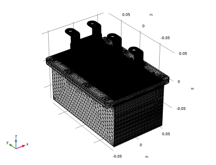
In the Model Builder window, right-click Mesh 1 and choose Build All, this might take a few minutes.
 |