PDF

Contact Impedance Comparison
Introduction
The contact impedance boundary condition is meant to approximate a thin layer of material that impedes the flow of current normal to the boundary, but does not introduce any additional conduction path tangential to the boundary. This example compares the contact impedance boundary condition to a full-fidelity model and discusses the range of applicability of this boundary condition.
Figure 1: A square two-dimensional domain of conductive material, with a circular inclusion. The wall of the inclusion is made of a material with lower conductivity.
Model Definition
The situation being modeled is shown in Figure 1. A square two-dimensional domain of conductive material has a DC voltage difference applied to it. Within the square domain, there is a circular inclusion. The walls of this inclusion are modeled two ways: using a full fidelity model that includes the thickness of the walls, and using the contact impedance boundary condition. The interior of the inclusion has the same properties as the bulk.
The location of the contact impedance condition is at the centerline, midway between the inner and outer radii of the full fidelity model. Note that, when using the contact impedance boundary condition, the total volume of the surrounding material is slightly larger, since the thickness of the wall is not being explicitly modeled. The conductivity of the wall of the inclusion is varied between a value several orders of magnitude smaller to a value equal to the conductivity of the bulk.
Results and Discussion
The voltage distribution and the current density norm is plotted in Figure 2 for the case where the electric conductivity is a thousand times smaller in the wall of the inclusion. This case represents a thin walled object that resists current flow through the surface, that is, it presents a high impedance to the voltage source. The field lines can be observed to deform around the object. The solutions agree well for the cases where the conductivity of the contact impedance boundary condition is less than the surrounding medium.
Figure 2: A surface plot of the current density norm, together with isolines of the electric potential and streamlines indicating the current direction, for the case of a thin layer of material that has a high impedance. The full fidelity and contact impedance solutions are almost identical.
The case of equal conductivities is plotted in Figure 3, and shows the limit of the contact impedance boundary condition. As the conductivities becomes equal, there can be no current flow tangential to the boundary.
Figure 3: A surface plot of the current density norm, together with isolines of the electric potential and streamlines indicating the current direction. The contact impedance boundary condition (right) prevents any tangential current flow and the solutions do not agree for this case.
The Contact Impedance boundary condition can be used in cases where the thickness of the boundary being approximated is much smaller than the characteristic size of the model domain, and when the conductivity of the layer is smaller than the surrounding medium. When this boundary condition can be used, the resulting number of mesh element is much smaller, saving solution time and memory.
Application Library path: ACDC_Module/Introductory_Electric_Currents/contact_impedance_comparison
Modeling Instructions
From the File menu, choose New.
New
In the New window, click  Model Wizard.
Model Wizard
1
In the Model Wizard window, click  2D.
2
In the Select Physics tree, select AC/DC > Electric Fields and Currents > Electric Currents (ec).
3
Click Add.
4
Click  Study.
5
In the Select Study tree, select General Studies > Stationary.
6
Global Definitions
Parameters 1
1
In the Model Builder window, under Global Definitions click Parameters 1.
2
In the Settings window for Parameters, locate the Parameters section.
3
Geometry 1
Square 1 (sq1)
1
In the Geometry toolbar, click  Square.
2
In the Settings window for Square, locate the Position section.
3
In the x text field, type 0.05.
Square 2 (sq2)
1
In the Geometry toolbar, click  Square.
2
In the Settings window for Square, locate the Position section.
3
In the x text field, type -1.05.
4
Click  Build All Objects.
5
Click the  Zoom Extents button in the Graphics toolbar.
Circle 1 (c1)
1
In the Geometry toolbar, click  Circle.
2
In the Settings window for Circle, locate the Size and Shape section.
3
In the Radius text field, type 0.245.
4
Locate the Position section. In the x text field, type 0.55.
5
In the y text field, type 0.5.
Circle 2 (c2)
1
In the Geometry toolbar, click  Circle.
2
In the Settings window for Circle, locate the Size and Shape section.
3
In the Radius text field, type 0.25.
4
Locate the Position section. In the x text field, type -0.55.
5
In the y text field, type 0.5.
6
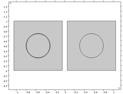
Click to expand the Layers section. In the table, enter the following settings:
Form Union (fin)
1
In the Geometry toolbar, click  Build All.
2
Click the  Zoom Extents button in the Graphics toolbar.
3
In the Model Builder window, click Form Union (fin).
The geometry on the left side describes the full fidelity model. The geometry on the right side replaces the thin layer with a boundary in order to use the Contact Impedance feature.
Create a set of selections for use before setting up the physics. First, create a selection for the wall of the inclusion.
Definitions
Full Fidelity
1
In the Definitions toolbar, click  Explicit.
2
3
In the Settings window for Explicit, type Full Fidelity in the Label text field.
Add a selection for the contact impedance boundaries.
Contact Impedance
1
In the Definitions toolbar, click  Explicit.
2
In the Settings window for Explicit, locate the Input Entities section.
3
From the Geometric entity level list, choose Boundary.
4
5
In the Label text field, type Contact Impedance.
Add a selection for the bulk area. These are the domains complementary to the wall of the inclusion.
Bulk
1
In the Definitions toolbar, click  Complement.
2
In the Settings window for Complement, locate the Input Entities section.
3
Under Selections to invert, click  Add.
4
In the Add dialog, select Full Fidelity in the Selections to invert list.
5
6
In the Settings window for Complement, type Bulk in the Label text field.
Electric Currents (ec)
Ground 1
1
In the Physics toolbar, click  Boundaries and choose Ground.
2
Ground 2
1
In the Physics toolbar, click  Boundaries and choose Ground.
2
Boundary Terminal 1
1
In the Physics toolbar, click  Boundaries and choose Boundary Terminal.
2
3
In the Settings window for Boundary Terminal, locate the Terminal section.
4
From the Terminal type list, choose Voltage.
Boundary Terminal 2
1
In the Physics toolbar, click  Boundaries and choose Boundary Terminal.
2
3
In the Settings window for Boundary Terminal, locate the Terminal section.
4
From the Terminal type list, choose Voltage.
Contact Impedance 1
1
In the Physics toolbar, click  Boundaries and choose Contact Impedance.
2
In the Settings window for Contact Impedance, locate the Boundary Selection section.
3
From the Selection list, choose Contact Impedance.
4
Locate the Contact Impedance section. In the ds text field, type 1[cm].
Materials
Material 1 (mat1)
1
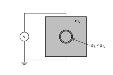
In the Model Builder window, under Component 1 (comp1) right-click Materials and choose Blank Material.
2
In the Settings window for Material, locate the Geometric Entity Selection section.
3
From the Selection list, choose Bulk.
4
Locate the Material Contents section. In the table, enter the following settings:
Material 2 (mat2)
1
Right-click Materials and choose Blank Material.
2
In the Settings window for Material, locate the Geometric Entity Selection section.
3
From the Selection list, choose Full Fidelity.
4
Locate the Material Contents section. In the table, enter the following settings:
Material 3 (mat3)
1
Right-click Materials and choose Blank Material.
2
In the Settings window for Material, locate the Geometric Entity Selection section.
3
From the Geometric entity level list, choose Boundary.
4
From the Selection list, choose Contact Impedance.
5
Locate the Material Contents section. In the table, enter the following settings:
Mesh 1
In the Model Builder window, under Component 1 (comp1) right-click Mesh 1 and choose Build All.
Study 1
Parametric Sweep
1
In the Study toolbar, click  Parametric Sweep.
2
In the Settings window for Parametric Sweep, locate the Study Settings section.
3
4
5
In the Study toolbar, click  Compute.
Begin the result analysis by excluding the interior of the wall of the inclusion which is not of interest.
Results
Study 1/Solution 1 (sol1)
In the Model Builder window, expand the Results > Datasets node, then click Study 1/Solution 1 (sol1).
Selection
1
In the Results toolbar, click  Attributes and choose Selection.
2
In the Settings window for Selection, locate the Geometric Entity Selection section.
3
From the Geometric entity level list, choose Domain.
4
From the Selection list, choose Bulk.
Create a custom plot to show the direction and norm of the current density.
Current Density (ec)
1
In the Results toolbar, click  2D Plot Group.
2
In the Settings window for 2D Plot Group, type Current Density (ec) in the Label text field.
Surface 1
1
Right-click Current Density (ec) and choose Surface.
2
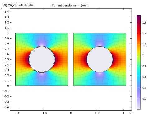
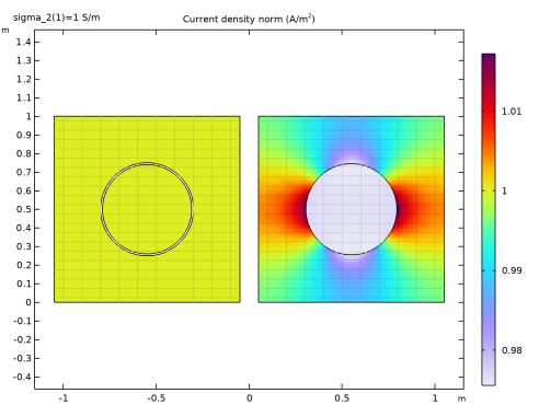
In the Settings window for Surface, click Replace Expression in the upper-right corner of the Expression section. From the menu, choose Component 1 (comp1) > Electric Currents > Currents and charge > ec.normJ - Current density norm - A/m².
3
Locate the Coloring and Style section. From the Color table list, choose Prism.
Next, add a contour plot showing the electric potential.
Contour 1
1
In the Model Builder window, right-click Current Density (ec) and choose Contour.
2
In the Settings window for Contour, click to expand the Title section.
3
From the Title type list, choose None.
4
Click to expand the Inherit Style section. From the Plot list, choose Surface 1.
5
Clear the Color checkbox.
Color Expression 1
1
Right-click Contour 1 and choose Color Expression.
2
In the Settings window for Color Expression, click Replace Expression in the upper-right corner of the Expression section. From the menu, choose ec.normJ - Current density norm - A/m².
3
Locate the Coloring and Style section. From the Color table list, choose PrismDark.
4
Clear the Color legend checkbox.
Then, add a streamline plot showing the current density.
Streamline 1
1
In the Model Builder window, right-click Current Density (ec) and choose Streamline.
2
3
Click the  Zoom Extents button in the Graphics toolbar.
4
In the Settings window for Streamline, click to expand the Title section.
5
From the Title type list, choose None.
6
Click to expand the Inherit Style section. From the Plot list, choose Surface 1.
7
Clear the Color checkbox.
Color Expression 1
In the Model Builder window, under Results > Current Density (ec) > Contour 1 right-click Color Expression 1 and choose Copy.
Color Expression 1
1
In the Model Builder window, right-click Streamline 1 and choose Paste Color Expression.
2
In the Current Density (ec) toolbar, click  Plot.
3
Click the  Zoom Extents button in the Graphics toolbar.
Compare the plot with Figure 2.
Current Density (ec)
1
In the Model Builder window, under Results click Current Density (ec).
2
In the Settings window for 2D Plot Group, locate the Data section.
3
From the Parameter value (sigma_2 (S/m)) list, choose 1.
4
In the Current Density (ec) toolbar, click  Plot.
This plot should look like Figure 3. Note that due to the selection defined in Solution 1, the streamlines in the full fidelity model are not completely visualized.