To add an Import node, from the
Home or
Geometry toolbar, click
Import (

). In the
Source section of the
Settings window, set the type of file to import to
ECAD file. You can also skip this step as the type of the selected file is automatically recognized. Click
Browse to locate the file to import, or enter the path to the file. Before clicking the
Import button consider to review and configure the import options, especially the layer thickness information, since in many cases the IPC-2581 files and ODB++ archives do not include all necessary information to construct a 3D geometry. If the content of the file have been changed which would affect the listed layers, nets or components in the settings, you can click
Refresh Data from File (

) button to get the new contents.
For PCB files, you can click the Preview (

) button in the
Settings window toolbar to show the preview of the file content in the
Graphics window. In the
Preview settings you can also control which layers and nets to add to import (
Controlling The Layer Stackup).
The length unit in the file is detected and displayed in the Settings window. To use the unit in the file as the length unit for the geometry sequence select the
Update geometry unit checkbox. The checkbox is selected by default if the
Import node is added as the first node in the geometry sequence. The length unit of the geometry sequence is set to
inch when the length unit
mil is detected in the selected file.
|
•
|
All. This alternative is available only in 3D. The import algorithm extrudes in one operation all imported copper and dielectric layers into a single 3D geometry object. From each copper layer, the imported symbols, such as lines, pads, and surfaces, are combined before extrusion. The copper and dielectric layers become domains in the resulting object. To be able to connect the layers, the algorithm requires that the 2D layouts fulfill certain rules. If the import fails, switch to the By layer grouping option.
|
|
•
|
By layer. Use this alternative to extrude each layer separately. The imported symbols, such as lines, pads, or surfaces, from the copper layers are combined before extrusion. Several geometry objects, one for each imported copper and dielectric layer, are generated upon import.
|
|
•
|
No grouping. Use this alternative to import and extrude individually each symbol from the copper layers. The import results in separate objects for imported symbols and dielectric layers. You can use this option if you want to manually delete certain objects after import, but it is recommended to do this only for relatively simple geometries.
|
When using the No grouping alternative you have the option to import line symbols as curve objects by selecting the
Ignore line width checkbox.
The Type of import list specifies whether copper layers are extruded or not by the import.
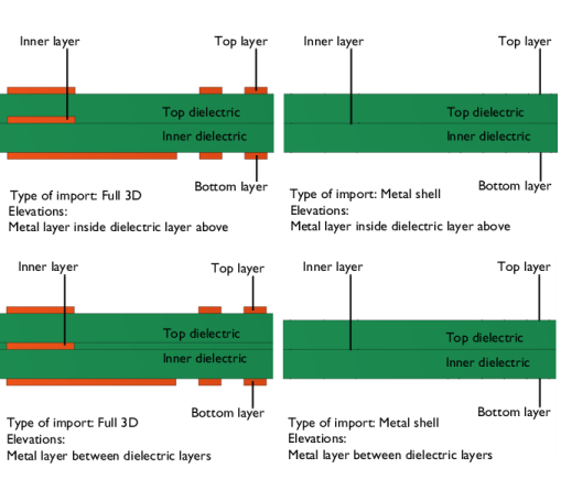
The Full 3D option imports all copper layers with a thickness according to the table in the
Layers section of the
Settings window. The layer elevations are determined according to
Elevations, see in the next section
Controlling The Layer Stackup. With the
Metal shell option copper layers are imported as embedded boundaries between dielectric regions. As illustrated in the figure above, switching to
Metal shell changes the elevation of dielectric layers when
Elevations is set to
Metal layer between dielectric layers.
|
|
For 3D imports, when the geometry grouping All and the import type Metal shell are used together, an isolated copper layer cannot be imported if the import also includes another solid (dielectric) layer. In this case use the By layer grouping, or add two Import features to the geometry sequence, one to import the copper layer, and a second one for the solid layers.
|
The import can read stackup information from the PCB file, such as the thickness for copper and dielectric layers. The layer information is displayed in the table in the Layers section of the
Settings window. Sometimes the layer thickness is not included in the export from the ECAD program, so the layers get the default zero thickness. Therefore it is recommended that these values are checked before importing.
|
•
|
Select Metal layer inside dielectric layer above to position interior copper layers inside the dielectric layer immediately above the copper layer. The layer elevations in the table are calculated automatically from the layer Thickness values. Using this option together with Type of Import set to Full 3D, the total thickness of the board is calculated as the sum of the dielectric layer thicknesses, plus the thickness of the top and bottom copper layers.
|
|
•
|
Select Metal layer between dielectric layers to position interior copper layers between the dielectric layers immediately below and above the copper layer. The layer elevations in the table are calculated automatically from the layer Thickness values. Using this option together with Type of Import set to Full 3D, all copper layers, including the interior copper layers, contribute to the total thickness of the circuit board, which is the sum of the thicknesses of all copper and dielectric layers. Extra dielectric layers are created for each copper layer at their respective z-extents and with the same shape as other dielectric layers to pad the gap between the main dielectrics. These are called in-layer dielectric.
|
|
•
|
Select Manual to enable the manual repositioning of layers in the stackup. The Elevation column appears in the table where you can enter values for the lower z positions of the layers. Any changes to the Elevation column in the table are lost when you switch to one of the other two options for Elevations. The Manual option is available only when Grouping of geometries is set to By layer or No grouping. 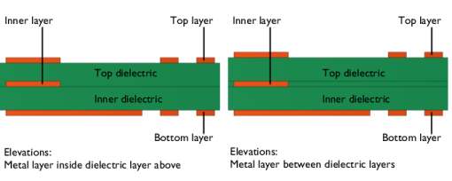
|
When Grouping of geometries is set to
By layer with the
Metal layer between dielectric layers option for calculating elevations, the checkbox
Unite metal layer and in-layer dielectric appears and is selected by default. If checkbox is selected, unites each copper layer with their respective in-layer dielectric. If checkbox is cleared, you get the copper and in-layer dielectric as separate objects.
Select the Show names from file checkbox to display the layer names as included in the PCB file. This is useful after assigning new layer names that are used in the COMSOL application.
|
•
|
The Name column displays the layer names from the file. You can edit the entries to give more descriptive names to the layers. The names that appear here are used to name the resulting geometry objects and the selections when the Layer selections checkbox is selected under Selections of Resulting Entities.
|
|
•
|
The Name in file column is visible only when you select the Show names from file checkbox above the table. The Name in file column always displays the layer name from the PCB file, even after editing the Name column.
|
|
•
|
The Type column declares the type of layers. Depending on their type, the import treats layers differently during import. For example, the geometry from a layer of type Metal is extruded only if the Type of import is set to Full 3D. Layers of type Dielectric are extruded, when selected in the Import column, according to the thickness and elevation data in the table. A union of the objects from the Outline layer is used as the PCB outline to determine the extent of the dielectric layers. The Drill layer type means that the objects in the layer define drilled holes in the PCB. ODB++ files may sometimes contain copper layers with the context set to MISC. These are displayed as layers of type Metal misc in the table, and they are by default not selected for import, similarly to layers of type Other.
|
|
•
|
The values in the Thickness column are used as the extrusion distances for the layers. The layer elevations are calculated based on these values unless the Elevation column is displayed. The values in the layer Thickness column can always be changed prior to import.
|
|
•
|
The values in the Elevation column control the lower z positions of the layers. By adjusting the values you can adjust the position of layers in the stackup. The Elevation column is only displayed when Elevations is set to Manual.
|
|
•
|
The Import column. Clear the checkbox for layers that do not need to be imported. You can also control which layers are imported by using the Preview.
|
To save the layers table to a text file, click the Save to File (

) button under the table. To load layer table information from a text file, click the
Load from File (

) button under the table. Only the editable data in the table is affected when loading from file. Layer data in the file that does not match the existing layers in the table is ignored. To reset the thickness and elevation values in the table to the last read data from the PCB file click the
Reset Thickness and Elevation (

) button. To select the
Import checkbox in the table for all copper and dielectric layers click the
Select All Metal and Dielectric Layers for Import (

) button. Click the
Clear All Imports (

) button to clear all checkboxes in the
Import column.
When importing PCBs, the available nets from the file are displayed in a list where you can choose which nets to import. When you click Import (

), under the source section, only the nets that are selected in the
Nets to import tree will be imported. For PCB files that contain a large number of nets it may help to filter the nets list to display only nets that you have selected to import by selecting the
Only list nets to import checkbox. You can also enter any text in the
Filter text box to only display the net nodes that match the filter. To easily select or clear all nets for import, click the
Select All (

) button to select all checkboxes and
Clear All (

) button to clear all checkboxes that are currently displayed in the list. A specific part of the PCB will only be imported if both it’s layer and net are selected to be imported. You can also control which nets are imported by using the
Preview.
Most printed circuit boards have three types of drilling holes: Plated Through Holes, Non-Plated Through Holes, and Vias. Choose from the Drill layer handling list (available only when the
Grouping of geometries is
By Layer) how to handle the drill holes specified in the file:
|
•
|
Modify layer objects (default) – This option unites/subtracts the drill layers with/from the layers it intersects. When this is selected, the following checkboxes appear:
|
|
-
|
Create domains for the cores of vias (selected by default). When this is selected, the cores of the vias become domains. When this is cleared, the cores of the vias become void.
|
|
-
|
Via cores through metal layers (cleared by default). When this is selected, the vias will go through the metal layers. When this is cleared, the vias will not affect the metal layers.
|
|
-
|
Create domains for the cores of plated holes (selected by default). When this is selected, the cores of the plated holes will become domains. When this is cleared, the cores of the plated holes will become void.
|
|
-
|
Plated hole cores through metal layers (selected by default). When this is selected, the plated holes will go through the metal layers. When this is cleared, the plated holes will not affect the metal layers.
|
|
-
|
Create domains for non-plated holes (cleared by default). When this is selected, the non-plated holes will become domains. When this is cleared, the non-plated holes will become void. Note that non-plated holes always go through all the layers.
|
|
•
|
Create separate objects — This option creates one object for each metal and dielectric layer the drill layers intersects. When this is selected, the following checkboxes appear:
|
|
-
|
Via cores through metal layers (cleared by default). When cleared, you get no objects for intersections of vias with metal layers.
|
|
-
|
Plated hole cores through metal layers (selected by default). When cleared, you get no objects for intersections of plated holes with metal layers. 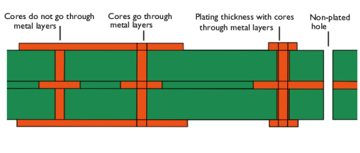
|
Specify the plating thickness of the plated holes and vias in the field Plating thickness (default 0) in 3D. When you set a positive thickness value, each drill hole will be surrounded by a cylindrical layer with the given thickness, except for non-plated drill holes. The plating will always be united with or become a part of the drill layer object. You will get no extra object for the plating if you choose
Create separate objects. Note that the plating thickness is also available if
Grouping of geometries is set to
No grouping, in which case the platings become separate objects from their respective cores.
When grouping of geometries is set to By layer or
No grouping, it is possible to choose to create only selected pads by selecting
From table (selected by default) option or
All, which creates all available pads. If
From table is chosen, a
Components to add list is shown, with all available components. Select components that you want to create pads for and click the
Add (

) button to add those components down to the table. In row in the table, in the
Component column, you specify one or more components for which the same pin numbers should be imported. It also supports entries such as
R* to consider all components whose names start with
R. The
Pins column lists the pin numbers from which pads should be created, for the chosen components in the same row. It is also possible to write
* to mean all pins for those components. Values in both columns should be separated with a comma or space. Use
Move Up (

),
Move Down (

) and
Delete (

) buttons to organize the table. Click the
Clear Table (

) button to clear all added pads from the table. To load pad table information from a text file, click the
Load from File button (

) under the table. To save the pads table to a text file, click the
Save to File button (

) under the table.
The pads will be assigned an attribute, where the value is <Component name>/<Pin number> and has the fields component, pin, net, package, and value. Read more about attributes in
Geometry Attributes. The attribute selects the pad on domain level or if doing a 3D import and the layer has thickness 0, on boundary level. The attribute tag is controlled in the text field
Pad attribute tag.
In a 3D geometry, you can specify whether the component should be represented by the extruded outline or by a surface as a 2D outline. From the Height of components list, select
From file (default) to extrude the 2D component outline to the height specified in the file. Select
Zero to import the component outline represented by a face.
Component outlines are positioned by default on the top copper layer or below the bottom copper layer. You can specify an offset for the vertical component placement in the Elevation offset for top components field for components on the top copper layer and the
Elevation offset for bottom components field for the components on the bottom copper layer.
The components will be assigned an attribute, where the values are the component names and are assigned to their respective component’s domain or surface (depending on if the component is 2D or 3D). This attribute also has the field “package” whose value is the package for each component. The attribute tag is controlled in the text field Component attribute tag. If there are multiple import features, their component attributes will be renamed after their respective import features, for example,
imp1.component and
imp2.component. If desired, these features could contribute to a single attribute by changing both attribute tags to have the same name, for example,
component.
By default the Keep interior boundaries checkbox is cleared to instruct the import to remove all interior boundaries on the imported layers. Interior boundaries on the copper layers are the result of the union of the individual symbols that make up the traces. Ignoring the interior boundaries keeps the geometry complexity to a minimum and can also make the import more robust in some situations.
Select the Ignore text objects checkbox to skip all objects in a PCB file that have the
TEXT tag set. To prevent objects outside the board from being imported select the checkbox
Ignore objects outside of board. Objects that are positioned outside the board, at a distance greater than that specified by the offset in the
Offset from boundary field, are ignored by the import. The default value for the offset is
−0.1 mm, which means that objects that are further into the board than 0.1 mm from the board boundary are imported. The offset should only be taken as an approximation. It is only checked where the object has its defining points, which are not necessarily the same points that can be seen on an object after it has been imported. For example, a trace is defined by its start and end points, which lie on the centerline of the trace. Similarly, a circle might be defined by four points (south, north, east, and west). Thus, an object might be ignored even if an edge is further inside the board than the specified offset, as long as all the points that define the object are farther away from the boundary than the offset.
Geometry repair is controlled via the Repair imported objects checkbox and the
Repair tolerance list. Change the
Repair tolerance from
Automatic to
Relative to manually specify a tolerance in the
Relative repair tolerance field.
Automatic means a relative repair tolerance of
10−6.
Select the Ignore vertices with continuous tangent checkbox (cleared by default), to remove, in each layer, vertices that connect two edges that have tangent directions making an angle less than the
Continuous tangent tolerance.
Select the Eliminate short edges checkbox (cleared by default) to eliminate edges that are shorter than the
Maximum edge length, by ignoring one or both of their adjacent vertices.
Select the Resulting objects selection checkbox to create predefined selections (for all levels — objects, domains, boundaries, edges, and points — that are applicable) in subsequent nodes in the geometry sequence. To also make all or one of the types of resulting entities (domains, boundaries, edges, and points) that the resulting objects consist of available as selections in all applicable selection lists (in physics and materials settings, for example), choose an option from the
Show in physics list:
All levels,
Domain selection,
Boundary selection,
Edge selection, or
Point selection. The default is
Domain selection, which is suitable for use with materials and physics defined in domains. For use with a boundary condition, for example, choose
Boundary selection. These selections do not appear as separate selection nodes in the model tree. Select
Off to not make any selection available outside of the geometry sequence.
Select the Layer selections checkbox to create predefined selections — for domains, boundaries, and objects — in subsequent nodes in the geometry sequence for each imported layer in the PCB file. The boundary selection for all layers include all boundaries of the objects.
Select the Net selections per layer checkbox to create domain and boundary net selections for each layer separately. When the checkbox is cleared, only net selections are generated and the intersection selections between net selections and all other selections generated from the import are not created during the import.
To make the resulting entities that the layers consist of available as selections in all applicable selection lists (in physics and materials settings, for example), choose an option from the Show in physics list:
All levels,
Domain selection, or
Boundary selection. The default is
All levels, which makes predefined selections available on all applicable levels, suitable for use with materials and physics defined in domains and boundaries. For use with a boundary condition, for example, choose
Boundary selection. These selections do not appear as separate selection nodes in the model tree. Select
Off to not make any selection available outside of the geometry sequence.
When the Layer selections checkbox is enabled, one selection will be created for each layer and for each geometric entity level, object, domain and boundary, for example:
SIG1, DIEL_1, GND, DIEL_2, SIG2.
For each DRILL layer, the following selections are available:
|
•
|
If the Plating thickness is zero:
|
|
-
|
When Create domains for the cores of vias or Create Separate objects is selected: A domain and a boundary selection for the vias, for example, DRILL.VIA. Note that boundary selection includes all the boundaries of the vias.
|
|
-
|
When Create domains for the cores of plated holes or Create separate objects is selected: A domain and a boundary selection for the plated holes, for example, DRILL.PLATED. Note that boundary selection includes all the boundaries of the plated holes.
|
|
-
|
When Create domains for non-plated holes or Create separate objects is selected: A domain and a boundary selection for the non-plated holes, for example, DRILL.NONPLATED. Note that boundary selection includes all the boundaries of the non-plated holes.
|
|
•
|
If the Plating thickness is positive:
|
|
-
|
When Create domains for the cores of vias or Create Separate objects is selected: A domain and a boundary selection for the vias, for example DRILL.VIA.CORE. Domain and boundary selections for the plating thickness of the vias, for example, DRILL.VIA.PLATING. Note that boundary selection includes all the boundaries of the vias.
|
|
-
|
When Create domains for the cores of plated holes or Create separate objects is selected: A domain and a boundary selection for the plated holes, for example, DRILL.PLATED.CORE. Domain and boundary selections for the plating thickness of the plated holes, for example DRILL.PLATED.PLATING. Note that boundary selection includes all the boundaries of the plated holes.
|
|
-
|
When Create domains for non-plated holes or Create separate objects is selected: A domain and a boundary selection for the non-plated holes, for example, DRILL.NONPLATED. Note that boundary selection includes all the boundaries of the non-plated holes.
|
When the checkbox Unite metal layer and in-layer dielectric is selected, the selections for all geometric levels are available for metal, for example INNER (which selects the entities corresponding to the metal). For the domain and boundary levels, in-layer dielectric selections are available, for example, INNER.ILDIEL (which selects entities corresponding to the dielectric). Note that the object selection is not available for in-layer dielectric. All boundary selections include all exterior boundaries of the layer.
When the checkbox Unite metal layer and in-layer dielectric is cleared, the selections for all geometric levels are available for both metal and dielectric, for example,
INNER (which selects the entities corresponding to the metal) and
INNER.ILDIEL (which selects entities corresponding to the dielectric).
If there are any pads selected for import, the Pads selection is created which selects the pads on domain level. If doing a 3D import and type of import is
Metal shell or the layer has zero thickness, the selection is created on a boundary level.
When the checkbox Import component outlines is selected, two selections are created for top and bottom components for all geometric levels (object, domain, and boundary), for example,
COMP_BOT and
COMP_TOP, referring to the bottom and top components, respectively.
Additionally, the import creates domain selection Metal, which selects all the metal layers. If there is no drill hole plating, the drill hole cores are also included, or if plating exists, it instead includes the plating domains. It does not include non-plated holes. The domain selection for
Dielectric selects everything else except the components. The boundary selection
Metal is always created and all exterior boundaries of the metal domains are selected.
If you want to make the resulting entities contribute to a cumulative selection, select a cumulative selection from the Contribute to list (the default,
None, gives no contribution), or click the
New button to create a new cumulative selection (see
Cumulative Selections in the
COMSOL Multiphysics Reference Manual).
The sections Domain Net Selections (in 2D and 3D) and
Boundary Net Selections (in 3D), contain a table that lists the generated selections for the imported nets. Net selections are generated when importing IPC-2581 and ODB++ files. The tables contain the following columns, ordered from left to right:
|
•
|
Name — This column contains the name of the selection.
|
|
•
|
Keep — The checkbox in this column is cleared by default, and determines whether the selection will be available for use in geometry features following the Import feature.
|
|
•
|
Physics — The checkbox in this column is selected by default. Provided that also the Keep checkbox has been selected, it determines whether the selection will be available in all applicable selection lists in physics and materials settings, for example. If the Import node has been added under the Plane Geometry node of a Work Plane, this column header is titled 3D. If the Import node has been added to a geometry part, this column header is titled Instances.
|
|
•
|
Contribute to — Select a cumulative selection from the list in this column to make the resulting entities contribute to a cumulative selection. The default, None, gives no contribution. Contributing to a cumulative selection does not require that the Keep checkbox has been selected.
|
Click the New Cumulative Selection button under the tables to create a new cumulative selection (see
Cumulative Selections in the
COMSOL Multiphysics Reference Manual).
The entities in a selection are highlighted in yellow in the Graphics window when the selection is clicked in the table. To zoom in on the selection use the
Zoom to Selection button in the
Graphics toolbar.
When the checkbox Net selections per layer is selected under the
Selection of Resulting Entities section, additional selection are created, one for each intersection between the net selections and all other selections generated from the import. This checkbox can be selected after the import has been done. For example, for the default behavior of the drill holes handling, importing a board with three copper layers (
SIG1,
GND,
SIG2), two dielectric layers (
SIG1_DIEL,
GND_DIEL), and one drill layer (
DRILL1), that contains a net named
NET, the following selections are generated:
NET, NET.SIG1,
NET.GND,
NET.SIG2,
NET.SIG1_DIEL, NET.GND_DIEL, NET.DRILL1_PLATED, NET.DRILL1_VIA, NET.Metal. Empty net selections are not generated; that is, a selection for the net is generated only when the intersection of the net and the layer contains entities. For entities that do not belong to a net, the selection
NONET is generated.
The selection NET is the union of all other selections for this net. If the name of a net is the same as the name of a layer, for example
GND, the suffix
_N is attached to the name of the net selection to avoid a name clash between net and layer selections. If pads have been selected for import, the net selections will also include
NET.Pads selection.
|
|
To view the list of all objects, you can use the Selection List window, that you can access from the Geometry toolbar. The top part of the Selection List window lists all geometry objects in the geometry sequence. The bottom part of the window lists all named selections, including the kept net selections.
|
For PCB files, you can click the Preview (

) button in the
Settings window toolbar to show the preview of the file content in the graphics. When clicked, the view is switched to preview mode, where the graphics switches to a 2D scene, and a window
Preview appears on the right side of the graphics. The preview rendering displays the metal and drill layers and consists of one object for each combination of layer and net, as well as the board outline as a curve object. The rendering shows the 2D geometries without any edges, and they are colored according to the layer they belong to.
The Preview settings window includes a section
Layers to Import, with a table listing the layers that are either metal layers or drill layers. The first column (

) controls the import of the layer while the second column (

) controls if the layer is displayed in the graphics. The third and fourth columns show the color and the name of each layer, respectively. When changing the value of the first column, an import checkbox (

), it automatically updates the corresponding checkbox in the
Layers table in the main import settings. This also affects the dielectric layer below, if such exists. The toolbar below the table contains shortcuts for easier manipulation of the table, like
Import All (

),
Import None (

),
Show All (

), and
Hide All (

) buttons. Right-clicking a row in a table brings up a context menu with actions that act on the selected rows. The actions are:
 Add to Import
,
 Remove from Import
,
 Hide
Hide,
 Show
Show, and
 Show Only This
, and they control the import of show checkboxes of the selected rows. Selecting a row in layers table marks the corresponding graphics objects in red. Additionally, there is a checkbox
Show board outline located below the table, which controls if the board’s outline is shown in the graphics.
The Nets to Import section contains a table equivalent to that in the
Layers to Import section, but acting on nets instead of layers. This table is also filterable, controlled with
Only list nets to import and
Only list visible nets checkboxes and a
Filter text field. The toolbar actions below the table only act on the rows currently displayed in the table. Selecting a row in the table will mark the corresponding graphics objects blue. At the top of the section is the checkbox
Select which nets to import in graphics. When this is selected you enter a mode where the objects that are selected in the graphics correspond to the objects that will be imported, that is, an object is selected if both its layer and net will be imported. In this mode, clicking in the graphics directly affects the
Nets to Import checkboxes, but only if the clicked object has its layer selected for import. Selecting a row in the table when in this mode marks the corresponding objects red, and those objects that are blue become green.
Hovering the mouse over an object will highlight it in red, but selecting it will select all objects belonging to the same net. The graphics context menu always contains the actions Select Box (

),
Zoom Box (

),
Zoom Extents (

),
Copy Image (

)and
Help (

). And if some objects are selected and the checkbox
Select which nets to import in graphics is cleared, it also contains the actions
 Add to Import
,
 Remove from Import
,
 Hide
Hide,
 Show Only This
, as well as
 Zoom to Selection
. The preview specific actions will act on the settings for the nets that the selected objects belong to.