|
1
|
|
2
|
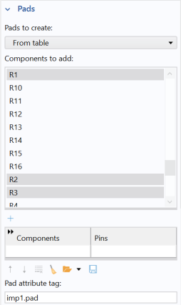
In the Components to add table hold Ctrl and select components C2, C4, C5, C6, R1, R2, R3.
|
|
7
|
In the Settings window for Import click the Browse button, then select the same file (printed_circuit_board_si_geom.zip) as previously.
|
|
12
|
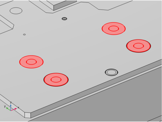
In the Logical expression text area, type imp2.component('C2','C4','C5','C6','R1','R2','R3').
|
 ) button.
 .
.
 .
. ) button. This will not import any layers of the board.
 .
. button in the Graphics toolbar.
 button in the Graphics toolbar.