View Settings
The extruded geometry of a circuit board can get quite complex, and due to the large thickness to width and length ratios of the layers it can be very difficult to see the structure after the import. Adjusting the view scaling in the Graphics window can help to get a better view, as well as hiding geometric entities, such as objects and faces, to be able to look inside the board structure.
1
Switch back from the Import settings window to the Model Builder window.
2
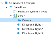
Under Component 1 expand first the Definitions and then the View 1 nodes.
3
Click the Camera node.
4
In the Settings window for Camera set the View scale to Manual. In the z scale text field, type 100.
Using this setting you can change the proportion of the geometry in all directions while the default no scaling sets the increments equal in all dimensions preserving the proportions of the geometry. You can also use Automatic settings, where the geometry fills the graphics window,.
5
Click Update
to refresh the view in the Graphics window.
6
To fit the entire board in the window click the Zoom Extents
button in the Graphics toolbar.
7
For less clutter turn off wireframe rendering by clicking the Wireframe Rendering button
.
You can now look inside the geometry for, example, by hiding the top dielectric layer.
8
Click
next to
Select Objects button from the Graphics toolbar, then choose
Select Domains. Next, click on the Click and Hide button
from the Graphics toolbar, then in the Graphics window click the domain marked in the figure to the right.
9
Click the Click and Hide button
again to deactivate hiding of selected objects. This is important in order to avoid hiding everything we click on in the Graphics window.
Note:
You can also view the hidden canvas by clicking the View Hidden Only button
.
 to refresh the view in the Graphics window.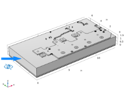
 button in the Graphics toolbar.
 .
. next to
  Select Objects button from the Graphics toolbar, then choose
  Select Domains. Next, click on the Click and Hide button
  from the Graphics toolbar, then in the Graphics window click the domain marked in the figure to the right.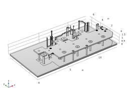
 again to deactivate hiding of selected objects. This is important in order to avoid hiding everything we click on in the Graphics window.
 .
.