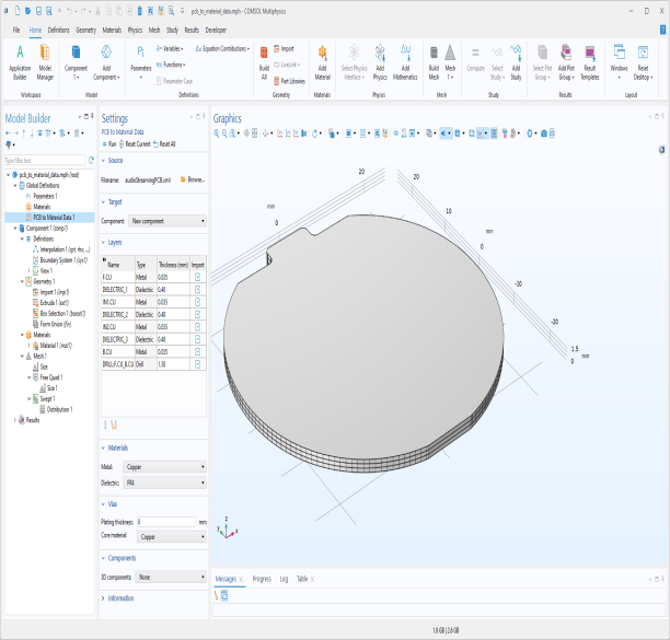
With the layout defined, the next step is to assign material properties. In the Materials section you decide how copper layers (including hole plating, if specified) and dielectric layers should be treated. While in the
Vias section, you can choose which materials will be assigned to via cores. The add-in supports both built-in materials and user-defined materials added to
Global Materials. Regardless of the choice, the assigned materials must contain a consistent set of six material properties: heat capacity, density, thermal conductivity, Young’s modulus, Poisson’s ratio, and coefficient of thermal expansion. These properties are essential for simulations involving heat transfer, solid mechanics, and thermal expansion. Note that only constant values are supported.
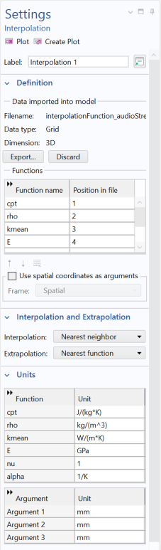 An interpolation function is defined by a file that provides function values at discrete grid points. In this workflow, an interpolation file is automatically generated by the add-in, with the naming convention interpolationFunction_<PCB
_
filename>. In the settings window for
Interpolation to the right you can see an example of an imported interpolation function file generated by the add-in. Six material properties (functions) are defined in the file:
cpt (heat capacity at constant pressure),
rho (density),
kmean (thermal conductivity),
E (Young’s modulus),
nu (Poisson’s ratio), and
alpha (coefficient of thermal expansion).
The Interpolation and
Extrapolation settings determine how values are evaluated between grid points and outside the defined coordinate domain. Both are set by default to
Nearest neighbor, meaning the value of the closest defined point is used. If required, these settings can be adjusted to other methods, depending on the needs of the analysis.
Finally, the Units section specifies the units of both the functions and their arguments. This table is generated automatically, with argument units derived from the geometry units defined in the PCB file.
To inspect the created interpolation function, you can click Create Plot in the settings toolbar. This generates a
3D Plot Group with slice plots of the function, similar to the example shown below. By default, the plot displays a low-resolution version of the interpolation data, but you can increase the level of detail by adjusting the grid resolution in the
3D Grid settings under
Datasets.
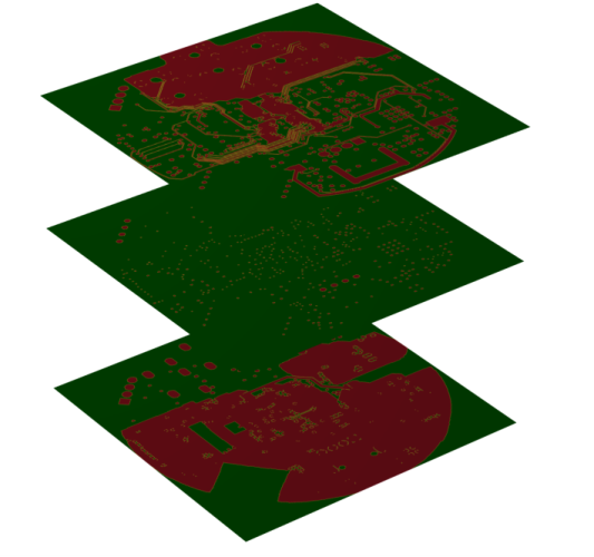
The PCB featured in the images originates from OtterCastAudioV2, Copyright © 2024 Ottercast, Jana Marie Hemsing, and it is made available under the
MIT license.
The toolbar at the top of the Settings window provides quick access to main controls of the add-in.
Click Run to execute the add-in and create an interpolation function representing the geometry of selected PCB. Click
Reset Current to reset only the options related to the currently selected board. Click
Reset All to restore all settings in the window to their defaults.
Use the Source section to select PCB. Click the
Browse button to open a file browser and select a PCB file you want to process.
The Target section defines where the interpolation function is created in the model. You can create a
New component (default) or insert the function into an already defined 3D component in the current model. The list shows all valid 3D components available for selection.
The Layers section provides a table that lists all metal, dielectric, and drill layers in the selected PCB. Each row contains the layer name, which can be renamed if needed, along with the layer type, such as metal, dielectric, or drill. The table also includes the thickness of each layer, with values that can be modified to match the desired board thickness. A set of checkboxes makes it possible to control whether individual layers are included in the analysis, with all layers selected for processing by default. For quick access, you can use buttons below table to
Clear all Layers or
Select All Layers.
In the Materials section, you can specify material properties for
Metal (including hole plating, if specified) and
Dielectric layers. The default option for metal is set to
Copper, while material for dielectric layers is set to
FR4. An alternative option is to set the layer material properties to an already defined material in the
Materials node under
Global Definitions.
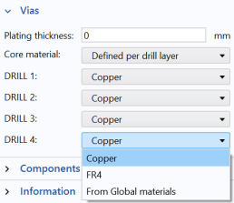
In the Vias section, you can assign material properties to the via cores. The core material can be set to
Copper or
FR4, or you can choose
From Global materials to assign material properties of an existing material in the
Materials node under
Global Definitions. It is also possible to add a plating to all holes by specifying the plating thickness.
When the selected file contains multiple drill layers, an additional Defined per drill layer option becomes available. This makes it possible to define core material properties individually for each drill layer.
The Components section controls how 3D PCB components are created in the target component. If
None is selected, no components are generated, while choosing
All creates every component included in the file.
Choosing Selected displays a table with all available components. By default, component import is turned off, but you can enable specific items by checking them in the table or by using the buttons below the table to select or clear all entries.
In the Information section, you will find the last build time, as well as the COMSOL Multiphysics version used to run the add-in.