Semiconductor Devices
The Semiconductor Module can be applied to solve a range of device simulation problems. The Semiconductor interface can be straightforwardly coupled with other physics interfaces, such as the Electromagnetic waves interfaces (using the predefined Semiconductor Optoelectronics multiphysics coupling), the Heat Transfer in Solids interface and the Electrical Circuits interface. Coupling to a circuit is straightforward using the terminals included with appropriate boundary conditions.
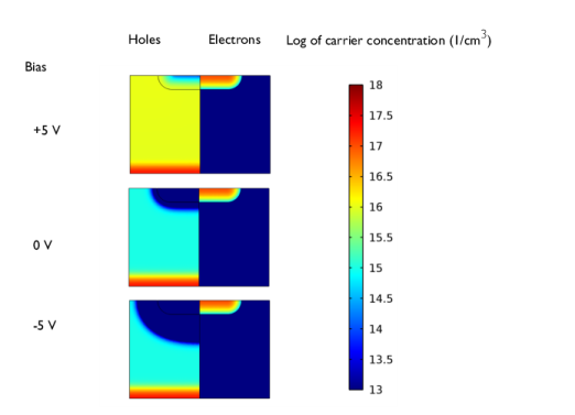
Figure 1
shows results obtained from a 2D p–n junction model in which a device model of a diode is coupled to an electrical circuit to produce a rectifier. The electron and hole concentrations are shown in the plots when different voltages are applied to the circuit.
Figure 1:
Electron and hole concentrations in a p–n junction diode connected to a series resistor under different bias conditions. This plot shows clearly the changing geometry and extent of the depletion region under reverse bias.
A range of common device types can be simulated with the module, including MOSFETs, MESFETs, JFETs, diodes, and bipolar transistors. These devices can be analyzed for the steady state, in the time domain or in the frequency domain (with mixed DC and AC signals, using the small signal analysis study type).
A number of standard analyses are illustrated with the MOSFET model series, which shows how to include a range of increasingly complicated semiconductor physics effects using features included within the Semiconductor interface. The first model in the MOSFET series is described in the section
Tutorial Model: DC Characteristics of a MOSFET
, below.
Figure 2
shows some of the results obtained from this analysis.
Figure 2:
Stationary analysis of a MOSFET. The plot shows the drain current plotted against the drain voltage (V
d
) for a range of different values of the gate voltage (V
g
) The inset shows the logarithm of the electron concentration (in units of cm
-3
) for a gate voltage of 4 V and for a drain voltage of 1 V. The channel is clearly visible.
In addition to the MOSFET model series, a wide array of other example models are available. The Bipolar Transistor model sequence gives an example of how to set up a multiphysics device simulation. Initially, a model of a 2D cross section of a bipolar transistor device is created using only the Semiconductor interface. This model is then extended by two other models in the sequence, one adds coupling to the Heat Transfer interface and the other demonstrates how to create a full 3D simulation of the same device.
The MOSCAP model series shows different ways of analyzing this fundamental building block of many devices. The ISFET model demonstrates the coupling to the electrochemistry physics. The Heterojunction Tunneling model shows how to add tunneling current contributions using the WKB approximation. The Interface Trapping Effects of A MOSCAP model does what its name suggests. The pair of models Reverse Recovery of a PIN Diode and Forward Recovery of a PIN Diode demonstrates the modeling of carrier dynamics with a time dependent study.
Several individual models are also provided, including a MESFET, an EEPROM device, a solar cell, a photodiode, and some LED models.
Figure 3
shows the electron and hole currents flowing in a simple 2D Bipolar transistor.
Figure 3:
Electric potential in V (color) and direction of the current flow for electrons (black arrows) and holes (white arrows) in a simple 2D bipolar transistor.
The density-gradient formulation is demonstrated in a 1D inversion layer, a 2D FET, and a 3D nanowire model. The last one is shown in
Figure 4
.
Figure 4:
Electron concentration (color), electric potential (isosurface), and total current density (arrow) of a 3D nanowire model with the quantum confinement effect included using the density-gradient formulation.
The Schrödinger Equation interface enables the modeling of various quantum-confined systems. The following graph shows the wave functions shifted by the respective energy levels for the resonant tunneling conditions of a double barrier structure.
The Schrödinger–Poisson Equation interface adds the Electrostatics physics to take into account the effects of the charge density of the carriers. The following graph shows the self-consistent result of electrons confined in a quantum wire.