|
|
|


|
1
|
|
2
|
|
3
|
Click Add.
|
|
4
|
|
5
|
Click Add.
|
|
6
|
In the Select Physics tree, select Optics > Wave Optics > Electromagnetic Waves, Frequency Domain (ewfd).
|
|
7
|
Click Add.
|
|
8
|
Click
|
|
9
|
|
10
|
Click
|
|
1
|
|
2
|
|
3
|
|
4
|
Browse to the model’s Application Libraries folder and double-click the file in_plane_switching_liquid_crystal_cell_general_parameters.txt.
|
|
1
|
|
2
|
|
3
|
|
4
|
Browse to the model’s Application Libraries folder and double-click the file in_plane_switching_liquid_crystal_cell_material_parameters.txt.
|
|
1
|
|
2
|
|
3
|
|
4
|
Browse to the model’s Application Libraries folder and double-click the file in_plane_switching_liquid_crystal_cell_geometry_parameters.txt.
|
|
1
|
|
2
|
|
3
|
|
4
|
|
5
|
|
6
|
Click to expand the Layers section. In the table, enter the following settings:
|
|
7
|
Select the Layers on top checkbox.
|
|
8
|
|
1
|
|
2
|
|
4
|
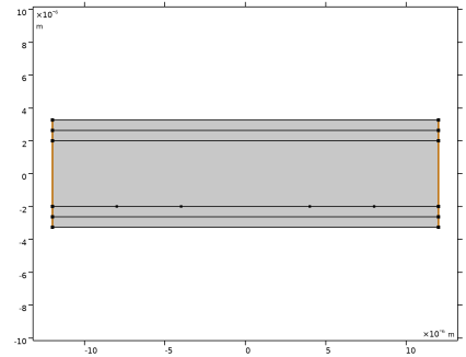
Locate the Selections of Resulting Entities section. Find the Cumulative selection subsection. Click New.
|
|
5
|
|
6
|
Click OK.
|
|
7
|
|
1
|
|
2
|
|
4
|
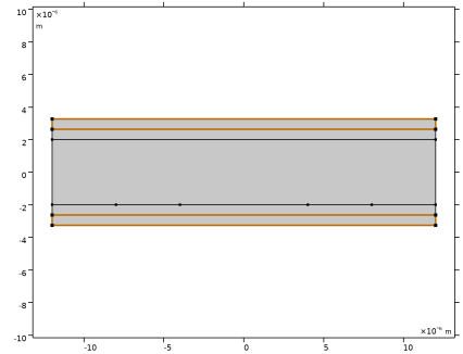
Locate the Selections of Resulting Entities section. Find the Cumulative selection subsection. Click New.
|
|
5
|
|
6
|
Click OK.
|
|
7
|
|
1
|
|
2
|
|
1
|
|
2
|
|
1
|
|
2
|
|
1
|
|
2
|
|
3
|
|
4
|
|
1
|
|
2
|
|
3
|
|
4
|
|
1
|
|
2
|
|
3
|
|
4
|
|
5
|
In the Add dialog, in the Selections to add list, choose Left Periodic Boundary and Right Periodic Boundary.
|
|
6
|
|
1
|
|
2
|
|
3
|
|
4
|
|
5
|
|
1
|
|
2
|
|
3
|
|
4
|
|
5
|
In the Add dialog, in the Selections to intersect list, choose Periodic Boundaries and PML Boundaries.
|
|
6
|
|
1
|
|
2
|
|
3
|
|
4
|
|
5
|
Click OK.
|
|
6
|
|
7
|
|
8
|
|
9
|
|
1
|
|
2
|
|
3
|
|
4
|
|
5
|
|
6
|
|
1
|
|
2
|
|
3
|
|
4
|
|
5
|
|
6
|
Browse to the model’s Application Libraries folder and double-click the file in_plane_switching_liquid_crystal_cell_domain_variables.txt.
|
|
1
|
|
2
|
|
3
|
|
4
|
|
5
|
|
6
|
|
7
|
Click OK.
|
|
8
|
|
9
|
|
10
|
In the Dependent variables (rad) table, enter the following settings:
|
|
1
|
|
2
|
|
3
|
|
4
|
|
1
|
|
2
|
In the Settings window for Dirichlet Boundary Condition, type Strong Anchoring in the Label text field.
|
|
4
|
|
5
|
|
1
|
|
2
|
|
3
|
|
1
|
|
2
|
|
3
|
|
1
|
|
2
|
|
3
|
|
4
|
Locate the Constitutive Relation D-E section. From the εr list, choose User defined. From the list, choose Symmetric.
|
|
5
|
|
1
|
|
2
|
|
3
|
|
1
|
|
2
|
|
3
|
|
4
|
|
1
|
|
2
|
|
3
|
|
1
|
|
2
|
|
3
|
|
1
|
|
1
|
In the Model Builder window, expand the Periodic Structure 1 node, then click Wave Equation, Electric 1.
|
|
2
|
|
3
|
|
1
|
In the Model Builder window, under Component 1 (comp1) right-click Materials and choose Blank Material.
|
|
2
|
|
3
|
|
4
|
Locate the Material Contents section. In the table, click to select the cell at row number 1 and column number 3.
|
|
5
|
|
6
|
|
8
|
Click OK.
|
|
9
|
|
1
|
|
2
|
|
3
|
|
4
|
Locate the Material Contents section. In the table, enter the following settings:
|
|
1
|
In the Model Builder window, under Component 1 (comp1) right-click Definitions and choose Variables.
|
|
2
|
In the Settings window for Variables, type Port Mode Field Polarization Variables in the Label text field.
|
|
3
|
|
4
|
|
5
|
|
6
|
Browse to the model’s Application Libraries folder and double-click the file in_plane_switching_liquid_crystal_cell_boundary_variables.txt.
|
|
1
|
In the Model Builder window, under Component 1 (comp1) > Electromagnetic Waves, Frequency Domain (ewfd) click Periodic Structure 1.
|
|
2
|
|
3
|
Click to select the
|
|
5
|
|
6
|
|
1
|
|
2
|
|
3
|
|
4
|
|
1
|
|
2
|
|
3
|
Click the Custom button.
|
|
4
|
Locate the Element Size Parameters section. In the Maximum element size text field, type lda0/n_e/6, to make sure that the electromagnetic wave is properly resolved.
|
|
1
|
|
2
|
|
3
|
|
4
|
|
1
|
|
2
|
|
3
|
|
4
|
|
1
|
|
2
|
|
1
|
|
2
|
|
3
|
Click
|
|
5
|
Click
|
|
6
|
|
7
|
|
8
|
|
9
|
Click Add.
|
|
10
|
|
11
|
Select the Reuse solution from previous step checkbox, to reduce the number of nonlinear iterations.
|
|
1
|
|
2
|
|
3
|
|
4
|
Locate the Physics and Variables Selection section. In the Solve for column of the table, under Component 1 (comp1), clear the checkboxes for Oseen-Frank (w) and Electrostatics (es).
|
|
5
|
|
1
|
|
2
|
|
3
|
|
4
|
|
1
|
|
2
|
|
3
|
Select the Show maximum and minimum values checkbox.
|
|
4
|
|
5
|
|
1
|
|
2
|
|
3
|
|
4
|
|
5
|
|
1
|
|
2
|
|
3
|
|
4
|
|
1
|
|
2
|
|
3
|
|
4
|
|
5
|
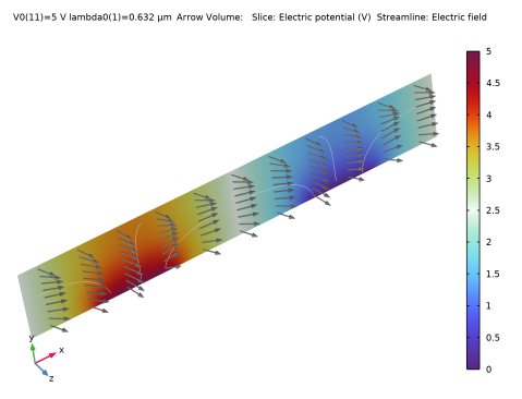
Locate the Arrow Positioning section. Find the x grid points subsection. In the Points text field, type 25.
|
|
1
|
|
2
|
|
3
|
|
4
|
|
5
|
|
6
|
|
7
|
|
8
|
|
1
|
|
2
|
|
3
|
|
1
|
|
2
|
|
3
|
|
1
|
|
2
|
|
3
|
|
4
|
|
5
|
|
1
|
|
2
|
|
1
|
|
2
|
|
3
|
|
1
|
|
2
|
|
3
|
|
4
|
|
5
|
|
6
|
|
1
|
|
2
|
|
3
|
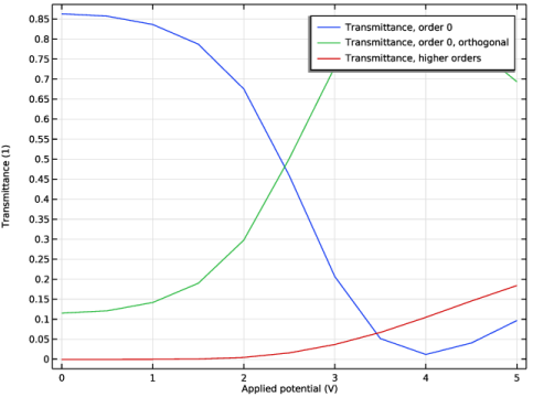
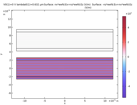
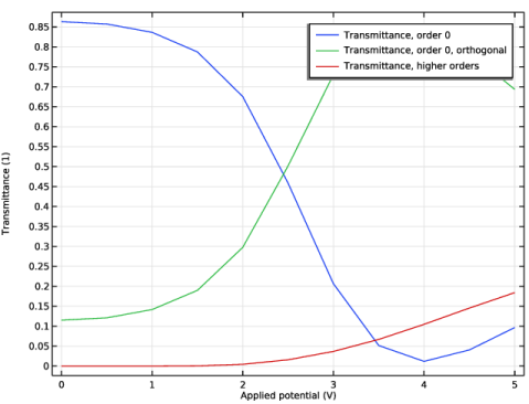
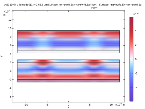
In the Expression text field, type nx*ewfd.Ex+nz*ewfd.Ez. This expression corresponds to the input field polarization.
|
|
4
|
|
1
|
|
2
|
|
3
|
In the Expression text field, type -nz*ewfd.Ex+nx*ewfd.Ez. This expression corresponds to a polarization orthogonal to the input field.
|
|
4
|
|
5
|
|
6
|
|
7
|
|
1
|
In the Model Builder window, under Results click Reflectance, Transmittance, and Absorptance (ewfd).
|
|
2
|
|
3
|
|
1
|
|
2
|
|
4
|
Click
|
|
5
|
|
6
|
|
7
|
|
1
|
|
2
|
|
3
|
|
1
|
|
2
|
|
1
|
|
2
|
|
3
|
Click to expand the Legends section. In the table, enter the following settings:
|
|
4
|
|
1
|
In the Model Builder window, expand the Study 1/Parametric Solutions 1 (4) (sol3) node, then click Selection.
|
|
2
|
|
3
|
|
1
|
|
2
|
|
3
|
|
4
|
|
1
|
|
2
|
|
1
|
|
2
|
|
3
|
|
4
|
|
5
|
|
6
|
Locate the Arrow Positioning section. Find the x grid points subsection. In the Points text field, type 11.
|
|
7
|
|
8
|
|
9
|
|
10
|
|
11
|
Click Define custom colors.
|
|
13
|
Click Add to custom colors.
|
|
14
|
|
1
|
|
2
|
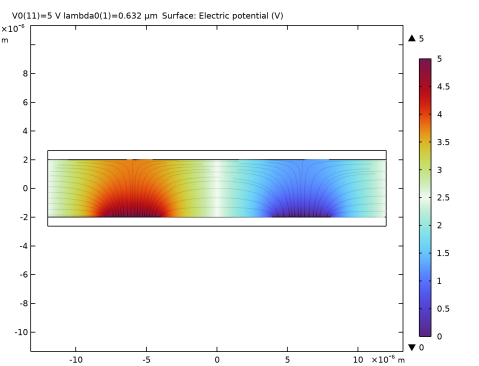
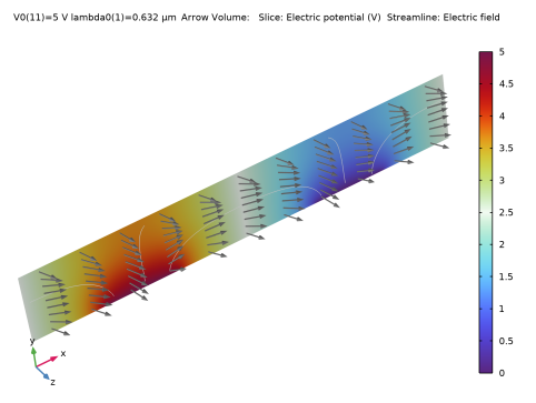
In the Settings window for Slice, click Replace Expression in the upper-right corner of the Expression section. From the menu, choose Component 1 (comp1) > Electrostatics > Electric > V - Electric potential - V.
|
|
3
|
|
4
|
|
5
|
|
1
|
|
2
|
|
3
|
Clear the Plot dataset edges checkbox.
|
|
4
|
|
1
|
|
2
|
In the Settings window for Streamline, click Replace Expression in the upper-right corner of the Expression section. From the menu, choose Component 1 (comp1) > Electrostatics > Electric > es.Ex,es.Ey,es.Ez - Electric field.
|
|
3
|
|
4
|
Locate the Coloring and Style section. Find the Point style subsection. From the Color list, choose Gray.
|
|
6
|