PDF

Tunnel Diode
Introduction
A tunnel diode, also known as an Esaki diode, is a heavily doped p–n junction diode with negative resistance due to tunneling, a quantum mechanical effect. A tunnel diode enables electrons to “tunnel” through the potential barrier at the junction, allowing for fast switching, which is beneficial in high-frequency applications.
At equilibrium, the Fermi levels of the p-type and n-type regions are aligned. By applying a forward bias, electrons can tunnel through the barrier due to the narrow depletion region. Therefore, electrons from the conduction band at the n-type region tunnel directly into the valence band of the p-type region. By raising the voltage further, the current reaches a peak value. After this point, the Fermi levels start to get misaligned and the tunneling current decreases, creating a negative resistance region. As the voltage continues to rise, the diode transitions to a standard operation, where current increases with voltage.
This model shows how to model the band-to-band tunneling effect in a tunnel diode.
Model Definition
This model employs a manual approach to simulate the tunneling effect in a tunnel diode. A User-Defined Recombination domain feature is used to make electrons disappear from the conduction band on the n-side and holes disappear from the valence band on the p-side, to mimic the effect of the electrons from the conduction band on the n-side tunneling into the valence band on the p-side. The rate of recombination can be computed with different levels of complexity. The current model takes the simplest approach as in Ref. 1, Section 8.2.1, where the tunneling current density is defined as
(1)
where the quantity Dt is an overlap integral, which modulates the shape of the I–V curve. It has the dimension of energy, depending on the temperature and the degeneracy, Vn and Vp, and is defined as
(2)
where FC(E) and FV(E) are the Fermi–Dirac distribution functions, ES is the smaller of the conduction and valence band energy levels, and is an energy-related component given by
(3)
The average electric field, ξ, is taken as half of the peak electric field from the simulation. The limits of the energy integration are also obtained from the numerical results.
The model is represented as a 1D domain with two 20 nm thick layers of highly n-doped and p-doped regions. The domains in which the electrons and holes disappear are selected in advance by visually estimating the approximate location where tunneling occurs. The recombination rates are assumed to be uniform within the domains.
The Modeling Instructions section describes the setup in detail.
Results and Discussion
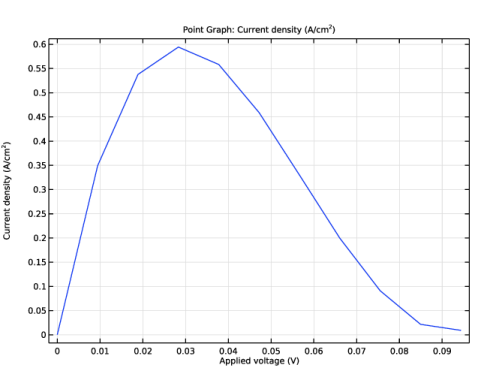
Figure 1 shows the current density versus applied voltage of the tunnel diode under forward bias. The plot shows the tunneling current increase at a low forward voltage, followed by the negative resistance region where tunneling decreases, leading to a drop in the current density.
Figure 1: Current density versus applied voltage of the tunnel diode.
Reference
1. S.M. Sze and K.K. Ng, Physics of Semiconductor Devices, 3rd ed., John Wiley & Sons, 2007.
Application Library path: Semiconductor_Module/Device_Building_Blocks/tunnel_diode
Modeling Instructions
From the File menu, choose New.
New
In the New window, click  Model Wizard.
Model Wizard
1
In the Model Wizard window, click  1D.
2
In the Select Physics tree, select Semiconductor > Semiconductor (semi).
3
Click Add.
4
Click  Study.
5
In the Select Study tree, select Preset Studies for Selected Physics Interfaces > Semiconductor Equilibrium.
6
Global Definitions
Parameters 1
1
In the Model Builder window, under Global Definitions click Parameters 1.
2
In the Settings window for Parameters, locate the Parameters section.
3
Geometry 1
Interval 1 (i1)
1
In the Model Builder window, under Component 1 (comp1) right-click Geometry 1 and choose Interval.
2
In the Settings window for Geometry, locate the Units section.
3
From the Length unit list, choose nm.
4
In the Model Builder window, click Interval 1 (i1).
5
In the Settings window for Interval, locate the Interval section.
6
Add Material
1
In the Materials toolbar, click  Add Material to open the Add Material window.
2
Go to the Add Material window.
3
In the tree, select Semiconductors > Ge - Germanium.
4
Click the Add to Component button in the window toolbar.
5
In the Materials toolbar, click  Add Material to close the Add Material window.
Definitions
Integration 1 (intop1)
1
In the Definitions toolbar, click  Nonlocal Couplings and choose Integration.
2
In the Settings window for Integration, type intop_p in the Operator name text field.
3
Locate the Source Selection section. From the Geometric entity level list, choose Boundary.
4
Integration 2 (intop_p2)
1
Right-click Integration 1 (intop_p) and choose Duplicate.
2
In the Settings window for Integration, type intop_n in the Operator name text field.
3
Locate the Source Selection section. Click  Clear Selection.
4
Integration 3 (intop_n2)
1
Right-click Integration 2 (intop_n) and choose Duplicate.
2
In the Settings window for Integration, type intop_0 in the Operator name text field.
3
Locate the Source Selection section. Click  Clear Selection.
4
Variables 1
1
In the Model Builder window, right-click Definitions and choose Variables.
2
In the Settings window for Variables, locate the Variables section.
3
Semiconductor (semi)
1
In the Model Builder window, under Component 1 (comp1) click Semiconductor (semi).
2
In the Settings window for Semiconductor, locate the Model Properties section.
3
From the Carrier statistics list, choose Fermi–Dirac.
Semiconductor Material Model 1
1
In the Model Builder window, under Component 1 (comp1) > Semiconductor (semi) click Semiconductor Material Model 1.
2
In the Settings window for Semiconductor Material Model, locate the Model Input section.
3
In the T text field, type T0.
Analytic Doping Model 1
1
In the Physics toolbar, click  Domains and choose Analytic Doping Model.
2
3
In the Settings window for Analytic Doping Model, locate the Impurity section.
4
In the NA0 text field, type Na.
Analytic Doping Model 2
1
Right-click Analytic Doping Model 1 and choose Duplicate.
2
In the Settings window for Analytic Doping Model, locate the Domain Selection section.
3
Click  Clear Selection.
4
5
Locate the Impurity section. From the Impurity type list, choose Donor doping (n-type).
6
In the ND0 text field, type Nd.
Here you can plot the preview of the doping profile for the p–n junction.
7
Click the Plot Net Doping Profile for All button in the window toolbar.
Metal Contact 1
1
In the Physics toolbar, click  Boundaries and choose Metal Contact.
2
Metal Contact 2
1
In the Physics toolbar, click  Boundaries and choose Metal Contact.
2
3
In the Settings window for Metal Contact, locate the Terminal section.
4
In the V0 text field, type V0.
Trap-Assisted Recombination 1
1
In the Physics toolbar, click  Domains and choose Trap-Assisted Recombination.
2
In the Settings window for Trap-Assisted Recombination, locate the Domain Selection section.
3
From the Selection list, choose All domains.
4
Locate the Shockley–Read–Hall Recombination section. From the τn list, choose User defined. From the τp list, choose User defined.
Define two User-Defined Recombination domain features. Use the first one to make electrons disappear from the conduction band on the n-side and the second one to make holes disappear from the valence band on the p-side. This mimics the band-to-band tunneling across a p–n junction. The domains where the electrons and holes disappear are defined approximately.
User-Defined Recombination 1
1
In the Physics toolbar, click  Domains and choose User-Defined Recombination.
2
3
In the Settings window for User-Defined Recombination, locate the User-Defined Recombination section.
4
In the Rn,0 text field, type Rt.
User-Defined Recombination 2
1
Right-click User-Defined Recombination 1 and choose Duplicate.
2
In the Settings window for User-Defined Recombination, locate the Domain Selection section.
3
Click  Clear Selection.
4
5
Locate the User-Defined Recombination section. In the Rn,0 text field, type 0[1/(m^3*s)].
6
In the Rp,0 text field, type Rt.
Mesh 1
1
In the Model Builder window, under Component 1 (comp1) click Mesh 1.
2
In the Settings window for Mesh, locate the Physics-Controlled Mesh section.
3
From the Element size list, choose Fine.
Study 1: Equilibrium
1
In the Model Builder window, click Study 1.
2
In the Settings window for Study, type Study 1: Equilibrium in the Label text field.
Step 1: Semiconductor Equilibrium
1
In the Model Builder window, under Study 1: Equilibrium click Step 1: Semiconductor Equilibrium.
2
In the Settings window for Semiconductor Equilibrium, locate the Study Settings section.
3
From the Tolerance list, choose User controlled.
4
In the Relative tolerance text field, type 1.0E-6.
5
In the Study toolbar, click  Compute.
Results
Evaluation Group 1
In the Results toolbar, click  Evaluation Group.
Point Evaluation 1
1
Right-click Evaluation Group 1 and choose Point Evaluation.
2
3
In the Settings window for Point Evaluation, locate the Expressions section.
4
Point Evaluation 2
1
In the Model Builder window, right-click Evaluation Group 1 and choose Point Evaluation.
2
3
In the Settings window for Point Evaluation, locate the Expressions section.
4
Evaluation Group 1
1
In the Model Builder window, click Evaluation Group 1.
2
In the Evaluation Group 1 toolbar, click  Evaluate.
Now take the evaluated values of Vn and Vp from the first study, as they reflect the degrees of the degeneracy of n+-side and p+-side, respectively.
Global Definitions
Parameters 2: from Result of Study 1 (Eval Group 1)
1
In the Home toolbar, click  Parameters and choose Add > Parameters.
2
In the Settings window for Parameters, type Parameters 2: from Result of Study 1 (Eval Group 1) in the Label text field.
3
Locate the Parameters section. In the table, enter the following settings:
Add Study
1
In the Home toolbar, click  Add Study to open the Add Study window.
2
Go to the Add Study window.
3
Find the Studies subsection. In the Select Study tree, select General Studies > Stationary.
4
Click the Add Study button in the window toolbar.
5
In the Home toolbar, click  Add Study to close the Add Study window.
Study 2: Sweep Vp
In the Settings window for Study, type Study 2: Sweep Vp in the Label text field.
Step 1: Stationary
1
In the Model Builder window, under Study 2: Sweep Vp click Step 1: Stationary.
2
In the Settings window for Stationary, locate the Study Settings section.
3
From the Tolerance list, choose User controlled.
4
In the Relative tolerance text field, type 1E-6.
5
Click to expand the Values of Dependent Variables section. Find the Initial values of variables solved for subsection. From the Settings list, choose User controlled.
6
From the Method list, choose Solution.
7
From the Study list, choose Study 1: Equilibrium, Semiconductor Equilibrium.
8
Click to expand the Study Extensions section. Select the Auxiliary sweep checkbox.
9
10
11
In the Study toolbar, click  Compute.
Results
Net Dopant Concentration (semi) 1
In the Model Builder window, under Results right-click Net Dopant Concentration (semi) 1 and choose Delete.
J-V
1
In the Results toolbar, click  1D Plot Group.
2
In the Settings window for 1D Plot Group, type J-V in the Label text field.
3
Locate the Data section. From the Dataset list, choose Study 2: Sweep Vp/Solution 2 (sol2).
Point Graph 1
1
Right-click J-V and choose Point Graph.
2
3
In the Settings window for Point Graph, locate the y-Axis Data section.
4
In the Expression text field, type semi.normJ.
5
In the Unit field, type A/cm^2.
6
Select the Description checkbox. In the associated text field, type Current density.
7
Locate the x-Axis Data section. From the Parameter list, choose Expression.
8
In the Expression text field, type V0.
9
Select the Description checkbox.
10
In the J-V toolbar, click  Plot.
Jx and Jt
1
In the Results toolbar, click  1D Plot Group.
2
In the Settings window for 1D Plot Group, type Jx and Jt in the Label text field.
3
Locate the Data section. From the Dataset list, choose Study 2: Sweep Vp/Solution 2 (sol2).
4
From the Parameter selection (V0) list, choose From list.
5
In the Parameter values (V0 (V)) list, select 0.037755.
Line Graph 1
1
Right-click Jx and Jt and choose Line Graph.
2
In the Settings window for Line Graph, locate the Selection section.
3
From the Selection list, choose All domains.
4
Locate the y-Axis Data section. In the Expression text field, type semi.JX.
5
In the Unit field, type A/cm^2.
6
Locate the x-Axis Data section. From the Parameter list, choose Expression.
7
In the Expression text field, type x.
8
Click to expand the Legends section. Select the Show legends checkbox.
9
Find the Include subsection. Clear the Solution checkbox.
10
Select the Description checkbox.
Line Graph 2
1
Right-click Line Graph 1 and choose Duplicate.
2
In the Settings window for Line Graph, locate the y-Axis Data section.
3
In the Expression text field, type Jt.
4
In the Jx and Jt toolbar, click  Plot.