PDF

Shockley Diode
Introduction
The Shockley diode is a four-layer semiconductor device with alternating P- and N-type semiconductor materials. Unlike conventional diodes, a Shockley diode has more than one p–n junction, forming a PNPN structure. The mode of operation for the Shockley diode is as follows: Upon a small-value forward bias, no current would flow due to the weak internal electric field to overcome the depletion region at the junction. Therefore, the device remains in its OFF state. When the forward bias exceeds a certain voltage, the depletion region shrinks, switching the device to turn ON and allowing current to flow. The Shockley diode remains in its ON state until the current drops and the device switches back to OFF.
The I–V curve of a Shockley diode typically has a loop. This means that a stationary study fails to compute the I–V curve because there are multiple solutions for a specific applied voltage. This model shows how to model a Shockley diode using a time-dependent study to obtain the I–V curve.
Model Definition
Figure 1 shows a 1D model of the PNPN structure of a Shockley diode together with the net doping concentration along the device. The device consists of four domains with alternating P- and N-doped domains defined by an Analytic Doping Model node. The electrodes are defined on both ends using a Metal Contact node. The cathode contact is grounded and a time-dependent voltage, based on a triangle function, is applied to the anode contact.
Figure 1: Net doping concentration along the PNPN structure of the Shockley diode, where the 1D-modeled device is shown at the bottom.
The Modeling Instructions section describes the setup in detail.
Results and Discussion
Figure 2 shows the I–V characteristics of the Shockley diode.
Figure 2: Current versus voltage characteristics of the Shockley diode.
Application Library path: Semiconductor_Module/Device_Building_Blocks/shockley_diode
Modeling Instructions
From the File menu, choose New.
New
In the New window, click  Model Wizard.
Model Wizard
1
In the Model Wizard window, click  1D.
2
In the Select Physics tree, select Semiconductor > Semiconductor (semi).
3
Click Add.
4
Click  Study.
5
In the Select Study tree, select Preset Studies for Selected Physics Interfaces > Semiconductor Equilibrium.
6
Global Definitions
Triangle 1 (tri1)
1
In the Home toolbar, click  Functions and choose Global > Triangle.
2
In the Settings window for Triangle, locate the Parameters section.
3
In the Lower limit text field, type 0.06.
4
In the Upper limit text field, type 0.94.
Parameters 1
1
In the Model Builder window, click Parameters 1.
2
In the Settings window for Parameters, locate the Parameters section.
3
Geometry 1
1
In the Model Builder window, under Component 1 (comp1) click Geometry 1.
2
In the Settings window for Geometry, locate the Units section.
3
From the Length unit list, choose µm.
Interval 1 (i1)
1
Right-click Component 1 (comp1) > Geometry 1 and choose Interval.
2
In the Settings window for Interval, locate the Interval section.
3
From the Specify list, choose Interval lengths.
4
Add Material from Library
In the Home toolbar, click  Windows and choose Add Material from Library.
Add Material
1
Go to the Add Material window.
2
In the tree, select Semiconductors > InP - Indium Phosphide.
3
Click the Add to Component button in the window toolbar.
Semiconductor (semi)
P Doping 1
1
In the Physics toolbar, click  Domains and choose Analytic Doping Model.
2
3
In the Settings window for Analytic Doping Model, type P Doping 1 in the Label text field.
4
Locate the Impurity section. In the NA0 text field, type 5e17[1/cm^3].
N Doping 2
1
Right-click P Doping 1 and choose Duplicate.
2
In the Settings window for Analytic Doping Model, type N Doping 2 in the Label text field.
3
Locate the Domain Selection section. Click  Clear Selection.
4
5
Locate the Impurity section. From the Impurity type list, choose Donor doping (n-type).
6
In the ND0 text field, type 2e17[1/cm^3].
P Doping 3
1
Right-click N Doping 2 and choose Duplicate.
2
In the Settings window for Analytic Doping Model, type P Doping 3 in the Label text field.
3
Locate the Domain Selection section. Click  Clear Selection.
4
5
Locate the Impurity section. From the Impurity type list, choose Acceptor doping (p-type).
6
In the NA0 text field, type 2e17[1/cm^3].
N Doping 4
1
Right-click P Doping 3 and choose Duplicate.
2
In the Settings window for Analytic Doping Model, type N Doping 4 in the Label text field.
3
Locate the Domain Selection section. Click  Clear Selection.
4
5
Locate the Impurity section. From the Impurity type list, choose Donor doping (n-type).
6
In the ND0 text field, type 5e17[1/cm^3].
Anode Contact
1
In the Physics toolbar, click  Boundaries and choose Metal Contact.
2
In the Settings window for Metal Contact, type Anode Contact in the Label text field.
3
4
Locate the Terminal section. In the V0 text field, type V0.
Cathode Contact
1
Right-click Anode Contact and choose Duplicate.
2
In the Settings window for Metal Contact, type Cathode Contact in the Label text field.
3
Locate the Boundary Selection section. Click  Clear Selection.
4
5
Locate the Terminal section. In the V0 text field, type 0[V].
Study 1
Step 2: Stationary
In the Study toolbar, click  Study Steps and choose Stationary > Stationary.
Step 3: Time Dependent
1
In the Study toolbar, click  Study Steps and choose Time Dependent > Time Dependent.
2
In the Settings window for Time Dependent, locate the Study Settings section.
3
From the Time unit list, choose ms.
4
In the Output times text field, type range(0,0.1,6).
5
In the Study toolbar, click  Compute.
Results
I-V Curve
1
In the Results toolbar, click  1D Plot Group.
2
In the Settings window for 1D Plot Group, type I-V Curve in the Label text field.
Global 1
1
Right-click I-V Curve and choose Global.
2
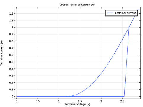
In the Settings window for Global, click Replace Expression in the upper-right corner of the y-Axis Data section. From the menu, choose Component 1 (comp1) > Semiconductor > Terminals > semi.I0_1 - Terminal current - A.
3
Click Replace Expression in the upper-right corner of the x-Axis Data section. From the menu, choose Component 1 (comp1) > Semiconductor > Terminals > semi.V0_1 - Terminal voltage - V.
4
In the I-V Curve toolbar, click  Plot.