|
|
|


|
1
|
|
2
|
In the Select Physics tree, select Radio Frequency > Electromagnetic Waves, Boundary Elements (embe).
|
|
3
|
Click Add.
|
|
4
|
Click
|
|
5
|
|
6
|
Click
|
|
1
|
|
2
|
|
3
|
|
1
|
|
2
|
|
3
|
|
4
|
|
5
|
|
6
|
|
1
|
|
2
|
|
3
|
|
4
|
|
1
|
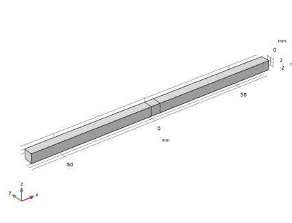
In the Model Builder window, under Component 1 (comp1) click Electromagnetic Waves, Boundary Elements (embe).
|
|
2
|
In the Settings window for Electromagnetic Waves, Boundary Elements, locate the Domain Selection section.
|
|
3
|
|
1
|
|
2
|
|
4
|
|
5
|
|
6
|
|
7
|
|
8
|
|
1
|
|
1
|
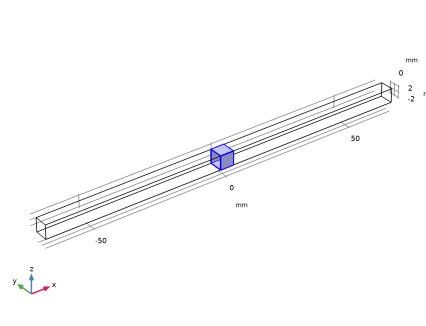
In the Model Builder window, under Component 1 (comp1) right-click Materials and choose Blank Material.
|
|
2
|
|
3
|
|
4
|
Locate the Material Contents section. In the table, enter the following settings:
|
|
1
|
|
2
|
Go to the Add Material window.
|
|
3
|
|
4
|
Click the Add to Component button in the window toolbar.
|
|
5
|
|
1
|
|
2
|
|
1
|
|
2
|
|
3
|
|
4
|
|
5
|
|
6
|
|
7
|
|
8
|
|
9
|
|
1
|
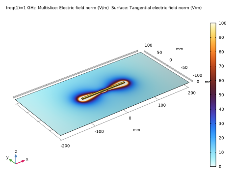
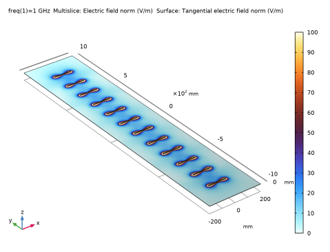
In the Model Builder window, expand the Results > Electric Field, Domains (embe) node, then click Multislice 1.
|
|
2
|
|
3
|
|
4
|
|
5
|
|
6
|
|
7
|
|
8
|
|
1
|
|
2
|
|
3
|
|
4
|
|
5
|
|
1
|
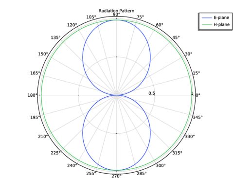
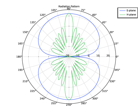
In the Model Builder window, expand the Results > 2D Far Field (embe) node, then click Radiation Pattern 1.
|
|
2
|
|
3
|
|
1
|
|
2
|
|
3
|
|
4
|
|
5
|
|
6
|
|
7
|
Locate the Legends section. In the table, enter the following settings:
|
|
8
|
|
1
|
|
2
|
|
3
|
|
4
|
|
1
|
|
2
|
|
1
|
|
2
|
|
3
|
|
4
|
|
5
|
|
1
|
|
2
|
|
4
|
Click
|
|
1
|
|
2
|
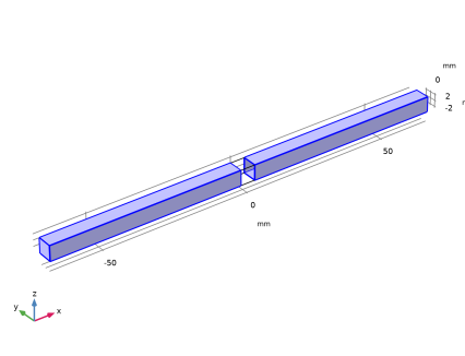
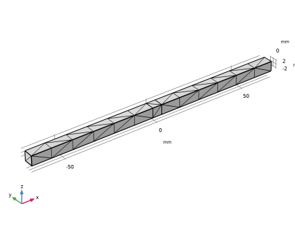
Click in the Graphics window and then press Ctrl+A to select both objects.
|
|
3
|
|
4
|
|
1
|
|
2
|
Click in the Graphics window and then press Ctrl+A to select both objects.
|
|
3
|
|
4
|
|
5
|
|
6
|
Click
|
|
7
|
|
1
|
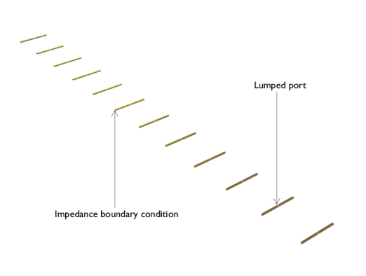
In the Model Builder window, under Component 1 (comp1) > Electromagnetic Waves, Boundary Elements (embe) click Lumped Port 1.
|
|
2
|
In the Settings window for Lumped Port, click the Split by Connectivity button in the window toolbar.
|
|
1
|
|
2
|
Go to the Add Study window.
|
|
3
|
|
4
|
Click the Add Study button in the window toolbar.
|
|
5
|
|
1
|
|
2
|
|
3
|
|
4
|
|
5
|
|
6
|
|
7
|
|
8
|
|
9
|
|
10
|
|
1
|
In the Model Builder window, expand the Results > Electric Field, Domains (embe) 1 node, then click Multislice 1.
|
|
2
|
|
3
|
|
4
|
|
5
|
|
6
|
|
7
|
|
8
|
|
1
|
|
2
|
|
3
|
|
4
|
|
5
|
|
1
|
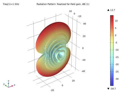
In the Model Builder window, expand the Results > 2D Far Field (embe) 1 node, then click Radiation Pattern 1.
|
|
2
|
|
3
|
|
4
|
|
5
|
|
6
|
|
8
|
|
1
|
|
2
|
|
3
|
|
4
|
|
5
|
|
6
|
|
7
|
Locate the Legends section. In the table, enter the following settings:
|
|
8
|
|
1
|
|
2
|
|
3
|
Select the Manual axis limits checkbox.
|
|
4
|
|
5
|
|
1
|
|
2
|
|
3
|
|
1
|
|
2
|
|
3
|
|
4
|
|
5
|
|
1
|
|
2
|
|
3
|
|
4
|
|
1
|
|
2
|
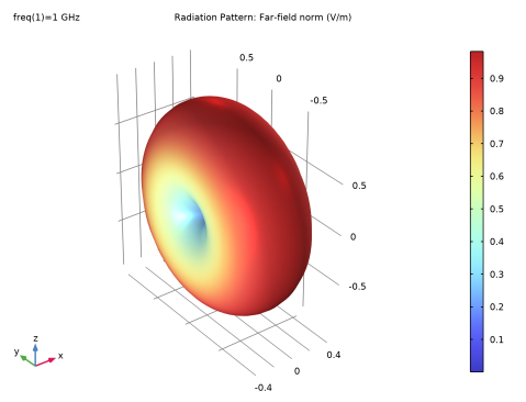
In the Settings window for Radiation Pattern, click Replace Expression in the upper-right corner of the Expression section. From the menu, choose Component 1 (comp1) > Electromagnetic Waves, Boundary Elements > Far field > embe.rGaindBEfar - Realized far-field gain, dBi - 1.
|
|
3
|
Locate the Expression section.
|
|
4
|
|
5
|
Locate the Evaluation section. Find the Angles subsection. In the Number of elevation angles text field, type 180.
|
|
6
|
|
7
|
|
8
|
|
1
|
|
2
|
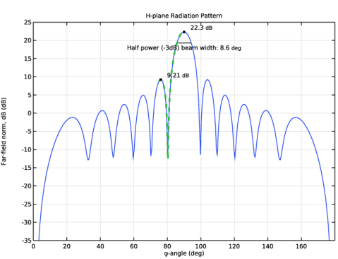
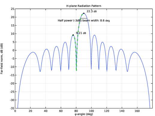
In the Settings window for 1D Plot Group, type 2D Far-Field, Dipole Array, H-Plane in the Label text field.
|
|
3
|
|
4
|
|
5
|
|
6
|
|
7
|
|
8
|
|
1
|
|
2
|
|
3
|
|
4
|
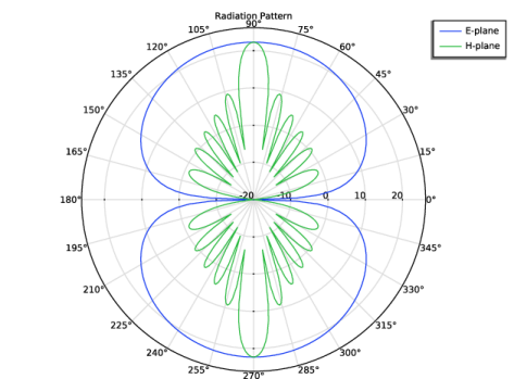
Locate the Evaluation section. Find the Angles subsection. In the Number of angles text field, type 360.
|
|
5
|
|
6
|
|
7
|
|
8
|
|
9
|
|
10
|
|
11
|
|
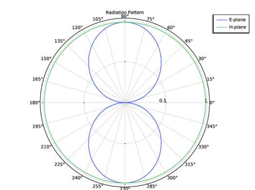
1
|
|
2
|
|
3
|
|
4
|
|
5
|
Click to expand the Coloring and Style section. Locate the Text Format section. In the Precision text field, type 2.
|
|
6
|
Select the Include unit checkbox.
|
|
7
|
|
8
|
|
9
|
|
10
|
|
1
|
In the Model Builder window, under Results > 2D Far-Field, Dipole Array, H-Plane right-click Radiation Pattern 1 and choose Duplicate.
|
|
2
|
|
3
|
|
4
|
|
5
|
Click to expand the Coloring and Style section. Find the Line style subsection. From the Line list, choose Dotted.
|
|
6
|
|
7
|
|
1
|
|
2
|
|
3
|
|
4
|
|
5
|
|
6
|
|
7
|
Clear the Prefix text field.
|
|
8
|
|
1
|
|
2
|
|
3
|
|
4
|
|
5
|