|
|
|
 |
 |


|
1
|
|
2
|
In the Select Physics tree, select Structural Mechanics > Electromagnetics–Structure Interaction > Piezoresistivity > Piezoresistivity, Boundary Currents.
|
|
3
|
Click Add.
|
|
4
|
Click
|
|
5
|
|
6
|
Click
|
|
1
|
|
2
|
|
3
|
|
4
|
|
5
|
Browse to the model’s Application Libraries folder and double-click the file piezoresistive_pressure_sensor_geom_sequence.mph.
|
|
6
|
|
7
|
|
8
|
|
1
|
|
2
|
|
3
|
|
1
|
|
2
|
Go to the Add Material window.
|
|
3
|
|
4
|
Right-click and choose Add to Component 1 (comp1).
|
|
5
|
|
6
|
Right-click and choose Add to Component 1 (comp1).
|
|
7
|
|
1
|
|
2
|
|
3
|
|
1
|
In the Model Builder window, under Component 1 (comp1) > Solid Mechanics (solid) click Linear Elastic Material 1.
|
|
2
|
|
3
|
|
4
|
|
5
|
|
1
|
|
2
|
|
3
|
|
1
|
|
2
|
|
3
|
|
4
|
|
5
|
|
1
|
|
2
|
|
3
|
|
4
|
|
5
|
|
6
|
In the Show More Options dialog, in the tree, select the checkbox for the node Physics > Advanced Physics Options.
|
|
7
|
Click OK.
|
|
1
|
In the Model Builder window, under Component 1 (comp1) > Electric Currents in Shells (ecis) click Conductive Shell 1.
|
|
2
|
|
3
|
|
4
|
Locate the Coordinate System Selection section. From the Coordinate system list, choose Rotated System 2 (sys2).
|
|
1
|
|
2
|
|
3
|
|
4
|
|
5
|
Locate the Coordinate System Selection section. From the Coordinate system list, choose Rotated System 2 (sys2).
|
|
1
|
|
1
|
|
3
|
|
4
|
|
5
|
|
1
|
|
1
|
|
1
|
|
2
|
|
3
|
From the list, choose User-controlled mesh.
|
|
1
|
|
2
|
|
3
|
Click the Custom button.
|
|
4
|
|
5
|
|
1
|
|
2
|
|
3
|
|
4
|
|
5
|
|
6
|
Locate the Element Size Parameters section.
|
|
7
|
|
8
|
|
1
|
|
2
|
|
3
|
|
4
|
|
1
|
|
2
|
|
3
|
|
5
|
|
1
|
|
2
|
|
3
|
|
1
|
|
2
|
Click
|
|
3
|
|
1
|
|
2
|
|
1
|
|
2
|
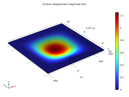
In the Settings window for Surface, click Replace Expression in the upper-right corner of the Expression section. From the menu, choose Component 1 (comp1) > Solid Mechanics > Displacement > solid.disp - Displacement magnitude - m.
|
|
1
|
|
2
|
|
1
|
|
2
|
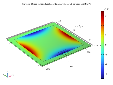
In the Settings window for 3D Plot Group, type In-Plane Shear Stress (Local Coordinates) in the Label text field.
|
|
1
|
|
2
|
In the Settings window for Surface, click Replace Expression in the upper-right corner of the Expression section. From the menu, choose Component 1 (comp1) > Solid Mechanics > Stress > Stress tensor, local coordinate system - N/m² > solid.slGp12 - Stress tensor, local coordinate system, 12-component.
|
|
3
|
|
1
|
|
2
|
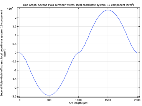
In the Settings window for 1D Plot Group, type In-Plane Shear Stress (Local Coordinate System) in the Label text field.
|
|
1
|
|
3
|
In the Settings window for Line Graph, click Replace Expression in the upper-right corner of the y-Axis Data section. From the menu, choose Component 1 (comp1) > Solid Mechanics > Stress > Second Piola–Kirchhoff stress, local coordinate system - N/m² > solid.SlGp12 - Second Piola–Kirchhoff stress, local coordinate system, 12-component.
|
|
4
|
|
1
|
|
2
|
|
1
|
|
2
|
|
3
|
|
4
|
|
5
|
Click
|
|
6
|
|
1
|
|
2
|
|
3
|
|
1
|
|
2
|
|
3
|
|
4
|
|
5
|
|
6
|
|
1
|
|
2
|
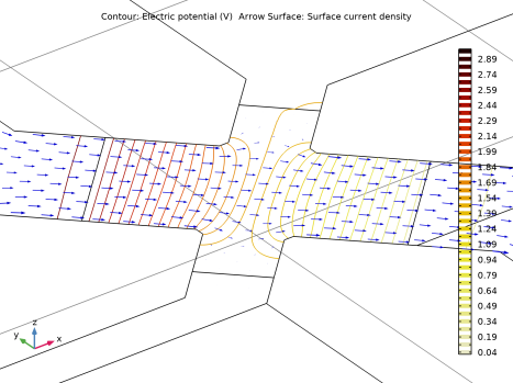
In the Settings window for Arrow Surface, click Replace Expression in the upper-right corner of the Expression section. From the menu, choose Component 1 (comp1) > Electric Currents in Shells > Currents and charge > ecis.JsX,...,ecis.JsZ - Surface current density (material and geometry frames).
|
|
3
|
Locate the Expression section.
|
|
4
|
|
5
|
Locate the Coloring and Style section.
|
|
6
|
|
7
|
|
8
|
|
9
|
|
1
|
|
2
|
In the Settings window for Global Evaluation, click Replace Expression in the upper-right corner of the Expressions section. From the menu, choose Component 1 (comp1) > Electric Currents in Shells > Terminals > ecis.I0_1 - Terminal current - A.
|
|
3
|
Click Add Expression in the upper-right corner of the Expressions section. From the menu, choose Component 1 (comp1) > Electric Currents in Shells > Terminals > ecis.V0_2 - Terminal voltage - V.
|
|
4
|
Locate the Expressions section. In the table, enter the following settings:
|
|
5
|
Click
|
|
1
|
|
2
|
|
1
|
|
2
|
|
3
|
|
4
|
|
5
|
|
6
|
Click to expand the Layers section. In the table, enter the following settings:
|
|
7
|
Select the Layers to the left checkbox.
|
|
8
|
Select the Layers to the right checkbox.
|
|
9
|
Select the Layers on top checkbox.
|
|
1
|
|
2
|
|
3
|
|
4
|
|
1
|
|
2
|
|
3
|
|
4
|
|
5
|
|
6
|
|
7
|
Click to expand the Layers section. In the table, enter the following settings:
|
|
8
|
Select the Layers to the right checkbox.
|
|
9
|
Select the Layers to the left checkbox.
|
|
10
|
Clear the Layers on bottom checkbox.
|
|
1
|
Right-click Component 1 (comp1) > Geometry 1 > Work Plane 1 (wp1) > Plane Geometry > Rectangle 1 (r1) and choose Duplicate.
|
|
2
|
|
3
|
|
4
|
|
5
|
|
6
|
Locate the Layers section. In the table, enter the following settings:
|
|
1
|
|
2
|
|
3
|
|
4
|
|
5
|
|
6
|
|
1
|
|
2
|
|
3
|
|
4
|
|
5
|
|
6
|
|
1
|
|
2
|
|
3
|
|
4
|
|
5
|
|
6
|
|
1
|
|
2
|
|
3
|
|
4
|
|
5
|
|
6
|
|
1
|
|
2
|
|
3
|
|
4
|
|
5
|
|
6
|
|
1
|
|
2
|
|
3
|
|
4
|
Select the Keep input objects checkbox.
|
|
1
|
In the Model Builder window, under Component 1 (comp1) > Geometry 1 right-click Work Plane 1 (wp1) and choose Extrude.
|
|
2
|
|
4
|
Select the Reverse direction checkbox.
|
|
1
|
|
2
|
|
3
|
|
4
|
On the object ext1, select Boundary 50 only.
|
|
5
|
In the tree, select ext1.
|
|
1
|
|
2
|
On the object fin, select Domains 10, 12, 14–18, 36, 39, 44–47, and 50 only.
|
|
1
|
|
2
|
On the object cmd1, select Domains 7, 12, 16, 18, 32, and 36–38 only.
|
|
1
|
|
2
|
On the object cmd2, select Domains 13, 14, 18–27, and 30 only.
|
|
1
|
|
2
|
On the object cmd3, select Domains 1–4, 6, and 23–25 only.
|
|
1
|
|
2
|
On the object cmd4, select Boundaries 23 and 109 only.
|
|
3
|
|
4
|
|
1
|
|
2
|
|
3
|
|
4
|
On the object parf1, select Boundary 46 only.
|
|
1
|
|
2
|
|
3
|
|
4
|
On the object parf1, select Boundaries 14, 26, 39, 73, 77, and 81 only.
|
|
1
|
|
2
|
|
3
|
|
4
|
|
5
|
|
6
|
|
7
|
|
8
|
|
9
|
|
1
|
|
2
|
|
3
|
|
4
|
|
1
|
|
2
|
|
3
|
|
4
|
Select the Group by continuous tangent checkbox.
|
|
5
|
On the object parf1, select Boundaries 3, 8, 13, 17, 21, 25, 32, 38, 45, 51, 56, 61, 72, 76, 80, 84, 97, and 103 only.
|
|
1
|
|
2
|
|
3
|
|
4
|
Select the Group by continuous tangent checkbox.
|
|
5
|
On the object parf1, select Boundaries 4, 9, 14, 18, 22, 26, 33, 39, 46, 52, 57, 62, 73, 77, 81, 85, 98, and 104 only.
|
|
1
|
|
2
|
|
3
|
|
4
|
|
5
|
|
6
|
Click OK.
|
|
7
|
|
8
|
|
9
|
|
10
|
Click OK.
|
|
1
|
|
2
|
|
3
|
|
4
|
|
5
|
|
6
|
Click OK.
|