PDF

Inductance Matrix Calculation of PCB Coils
Introduction
PCB (printed-circuit board) coils are widely used in a variety of industrial applications such as micromotor and microelectronic devices. For an array of PCB coils, it is generally of interest to know the inductive coupling represented by the inductance matrix. This model demonstrates how to use the Magnetic Fields, Currents Only interface to compute the inductance matrix of an array of coils in a multilayer PCB, as shown in Figure 1.
Figure 1: The geometry of PCB coils.
Model Definition
The geometry of the coils is usually ‘open’; the modeling of a closed current loop is not of interest and is also not necessary. The Magnetic Fields, Currents Only interface can model such nondivergence-free currents. For more details, see Theory for the Magnetic Fields, Currents Only Interface in the AC/DC Module User’s Guide.
The PCB coils are modeled by the Conductor feature, which can be used to easily set up the current sources. With using the Split by Connectivity functionality, 12 coils can be automatically identified and the corresponding Conductor features are created. This greatly simplifies the steps to set up the physics interface. The model is solved with a Stationary Source Sweep with Initialization study, as well as with a Frequency Domain Source Sweep with Initialization study. Both of these are dedicated to computing the lumped inductance matrix.
Results and Discussion
Figure 2 shows the distribution of the magnetic flux density norm around the PCB coils when the 8th conductor is activated, in the stationary case. Figure 3 illustrates the corresponding inductance matrix of the PCB coils. Similar plots for the frequency domain solution, are shown in Figure 4 and Figure 5, respectively.
Figure 2: The distribution of the magnetic flux density norm around PCB coils, stationary solution.
Figure 3: Visualization of the inductance matrix of PCB coils, stationary solution.
Figure 4: The distribution of the magnetic flux density norm around PCB coils, frequency domain solution.
Figure 5: Visualization of the inductance matrix of PCB coils, frequency domain solution.
Application Library path: ACDC_Module/Devices,_Inductive/inductance_matrix_pcb_coils
Modeling Instructions
From the File menu, choose New.
New
In the New window, click  Model Wizard.
Model Wizard
1
In the Model Wizard window, click  3D.
2
In the Select Physics tree, select AC/DC > Electromagnetic Fields > Vector Formulations > Magnetic Fields, Currents Only (mfco).
3
Click Add.
4
Click  Study.
5
In the Select Study tree, select Preset Studies for Selected Physics Interfaces > Stationary Source Sweep with Initialization.
6
Geometry 1
1
In the Model Builder window, under Component 1 (comp1) click Geometry 1.
2
In the Settings window for Geometry, locate the Advanced section.
3
From the Geometry representation list, choose CAD kernel.
Import 1 (imp1)
Since the geometry used for the model is quite complicated, import the coils from an existing file. Then manually add some blocks around these coils in the geometry to simplify the postprocessing.
1
In the Geometry toolbar, click  Import.
2
In the Settings window for Import, locate the Source section.
3
From the Source list, choose COMSOL Multiphysics file.
4
In the Filename text field, type inductance_matrix_pcb_coils.mphbin.
5
Click  Import.
6
Locate the Selections of Resulting Entities section. Select the Resulting objects selection checkbox.
7
From the Show in physics list, choose All levels.
8
Click the  Transparency button in the Graphics toolbar.
Ground Boundaries
1
In the Geometry toolbar, click  Selections and choose Explicit Selection.
2
In the Settings window for Explicit Selection, locate the Entities to Select section.
3
From the Geometric entity level list, choose Boundary.
4
On the object imp1, select Boundaries 6, 16, 26, 36, 2502, 2504, 2506, and 2508 only.
5
In the Label text field, type Ground Boundaries.
Input Terminals
1
In the Geometry toolbar, click  Selections and choose Explicit Selection.
2
In the Settings window for Explicit Selection, locate the Entities to Select section.
3
From the Geometric entity level list, choose Boundary.
4
On the object imp1, select Boundaries 1, 11, 21, and 31 only.
5
In the Label text field, type Input Terminals.
Interior Terminals
1
In the Geometry toolbar, click  Selections and choose Explicit Selection.
2
In the Settings window for Explicit Selection, locate the Entities to Select section.
3
From the Geometric entity level list, choose Boundary.
4
On the object imp1, select Boundaries 1261, 1266, 1271, and 1276 only.
5
In the Label text field, type Interior Terminals.
Output Terminals
1
In the Geometry toolbar, click  Selections and choose Explicit Selection.
2
In the Settings window for Explicit Selection, type Output Terminals in the Label text field.
3
Locate the Entities to Select section. From the Geometric entity level list, choose Boundary.
4
On the object imp1, select Boundaries 2501, 2503, 2505, and 2507 only.
Union Selection 1 (unisel1)
1
In the Geometry toolbar, click  Selections and choose Union Selection.
2
In the Settings window for Union Selection, locate the Geometric Entity Level section.
3
From the Level list, choose Boundary.
4
Locate the Input Entities section. Click  Add.
5
In the Add dialog, in the Selections to add list, choose Input Terminals, Interior Terminals, and Output Terminals.
6
Block 1 (blk1)
1
In the Geometry toolbar, click  Block.
2
In the Settings window for Block, locate the Size and Shape section.
3
In the Width text field, type 5[cm].
4
In the Depth text field, type 6[cm].
5
In the Height text field, type 2[cm].
6
Locate the Position section. From the Base list, choose Center.
Work Plane 1 (wp1)
1
In the Geometry toolbar, click  Work Plane.
2
In the Settings window for Work Plane, locate the Plane Definition section.
3
In the z-coordinate text field, type -2[mm].
Partition Objects 1 (par1)
1
In the Geometry toolbar, click  Booleans and Partitions and choose Partition Objects.
2
3
In the Settings window for Partition Objects, locate the Partition Objects section.
4
From the Partition with list, choose Work plane.
Work Plane 2 (wp2)
1
In the Geometry toolbar, click  Work Plane.
2
In the Settings window for Work Plane, locate the Plane Definition section.
3
From the Plane list, choose yz-plane.
4
In the x-coordinate text field, type 7[mm].
Partition Objects 2 (par2)
1
In the Geometry toolbar, click  Booleans and Partitions and choose Partition Objects.
2
3
In the Settings window for Partition Objects, locate the Partition Objects section.
4
From the Partition with list, choose Work plane.
Work Plane 3 (wp3)
1
In the Geometry toolbar, click  Work Plane.
2
In the Settings window for Work Plane, locate the Plane Definition section.
3
From the Plane list, choose zx-plane.
4
In the y-coordinate text field, type 14.25[mm].
Partition Objects 3 (par3)
1
In the Geometry toolbar, click  Booleans and Partitions and choose Partition Objects.
2
3
In the Settings window for Partition Objects, locate the Partition Objects section.
4
From the Partition with list, choose Work plane.
Form Union (fin)
1
In the Geometry toolbar, click  Build All.
2
Click the  Go to Default View button in the Graphics toolbar.
3
In the Model Builder window, click Form Union (fin).
Magnetic Fields, Currents Only (mfco)
The geometry is now complete. Next, define coil selections for the physics interface to use. This is achieved by selecting all conductors, and then using the Split by Connectivity action. This generates a duplicate of the original feature for each connected component. By construction each conductor will be not adjacent to any other Conductor, but the selection can be further edited if necessary. Feeding boundary conditions to each Conductor will also be similarly set.
Conductor 1
1
In the Physics toolbar, click  Domains and choose Conductor.
2
In the Settings window for Conductor, locate the Domain Selection section.
3
From the Selection list, choose Import 1.
Ground 1
In the Physics toolbar, click  Attributes and choose Ground.
Terminal 1
1
In the Model Builder window, click Terminal 1.
2
In the Settings window for Terminal, locate the Boundary Selection section.
3
From the Selection list, choose Union Selection 1.
Ground 1
1
In the Model Builder window, click Ground 1.
2
In the Settings window for Ground, locate the Boundary Selection section.
3
From the Selection list, choose Ground Boundaries.
Conductor 12
In the Model Builder window, under Component 1 (comp1) > Magnetic Fields, Currents Only (mfco) right-click Conductor 1 and choose Split by Connectivity.
Definitions
Hide for Physics 1
1
In the Model Builder window, expand the Component 1 (comp1) > Definitions node.
2
Right-click View 1 and choose Hide for Physics.
3
In the Settings window for Hide for Physics, locate the Geometric Entity Selection section.
4
From the Geometric entity level list, choose Boundary.
5
Mesh 1
1
In the Model Builder window, under Component 1 (comp1) click Mesh 1.
2
In the Settings window for Mesh, locate the Physics-Controlled Mesh section.
3
From the Element size list, choose Coarser.
4
Click the  Go to Default View button in the Graphics toolbar.
5
Click the  Transparency button in the Graphics toolbar.
6
Click  Build All.
Materials
Material 1 (mat1)
1
In the Model Builder window, under Component 1 (comp1) right-click Materials and choose Blank Material.
2
In the Settings window for Material, locate the Geometric Entity Selection section.
3
From the Selection list, choose Import 1.
4
Locate the Material Contents section. In the table, enter the following settings:
Study 1
Using Show Default Solver it is possible to identify in advance some problems.
Solution 1 (sol1)
In the Study toolbar, click  Show Default Solver.
Magnetic Fields, Currents Only (mfco)
Four empty selections Ground are identified and they can be inspected and removed before solving.
Ground 1
1
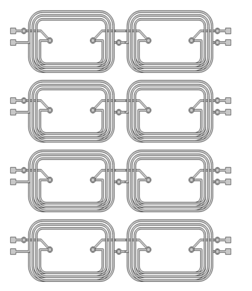
In the Model Builder window, under Component 1 (comp1) > Magnetic Fields, Currents Only (mfco) > Conductor Group 1, Ctrl-click to select Conductor 5 > Ground 1, Conductor 6 > Ground 1, Conductor 7 > Ground 1, and Conductor 8 > Ground 1.
2
Study 1
In the Study toolbar, click  Compute.
Results
Multislice 1
Now use the blocks around the coil geometry to create an illustration of the magnetic flux density norm. Remember to choose to solution where the coil that intersects the chosen planes is active.
1
In the Model Builder window, expand the Magnetic Flux Density (mfco) node, then click Multislice 1.
2
In the Settings window for Multislice, locate the Multiplane Data section.
3
Find the x-planes subsection. In the Coordinates text field, type 7[mm].
4
Find the y-planes subsection. In the Coordinates text field, type 14.25[mm].
5
Find the z-planes subsection. In the Coordinates text field, type -2[mm].
6
Click to expand the Range section. Select the Manual color range checkbox.
7
In the Maximum text field, type 8.0E-4.
Streamline Multislice 1
1
In the Model Builder window, click Streamline Multislice 1.
2
In the Settings window for Streamline Multislice, locate the Multiplane Data section.
3
Find the x-planes subsection. In the Coordinates text field, type 7[mm].
4
Find the y-planes subsection. In the Coordinates text field, type 14.25[mm].
5
Find the z-planes subsection. In the Coordinates text field, type -2[mm].
Magnetic Flux Density (mfco)
Right-click Results > Magnetic Flux Density (mfco) > Streamline Multislice 1 and choose Surface.
Surface 1
1
In the Settings window for Surface, locate the Expression section.
2
In the Expression text field, type 1.
Selection 1
1
Right-click Surface 1 and choose Selection.
2
In the Settings window for Selection, locate the Selection section.
3
From the Selection list, choose Import 1.
Material Appearance 1
1
Right-click Surface 1 and choose Material Appearance.
2
In the Settings window for Material Appearance, locate the Appearance section.
3
From the Appearance list, choose Custom.
4
From the Material type list, choose Copper.
Magnetic Flux Density Norm (DC)
1
In the Model Builder window, under Results click Magnetic Flux Density (mfco).
2
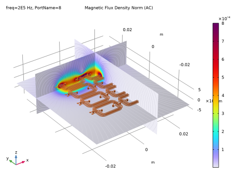
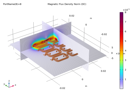
In the Settings window for 3D Plot Group, type Magnetic Flux Density Norm (DC) in the Label text field.
3
Locate the Data section. From the Parameter value (PortName) list, choose 8.
4
Click to expand the Title section. From the Title type list, choose Label.
5
Locate the Plot Settings section. Clear the Plot dataset edges checkbox.
6
Locate the Color Legend section. Clear the Show maximum and minimum values checkbox.
7
In the Magnetic Flux Density Norm (DC) toolbar, click  Plot.
Resistance (DC) (dset1, mfco)
1
In the Model Builder window, expand the Results > Lumped Parameters (dset1, mfco) node, then click Resistance (DC) (dset1, mfco).
2
In the Resistance (DC) (dset1, mfco) toolbar, click  Evaluate.
Inductance (DC) (dset1, mfco)
1
In the Model Builder window, click Inductance (DC) (dset1, mfco).
2
In the Inductance (DC) (dset1, mfco) toolbar, click  Evaluate.
The inductance matrix is shown in the table, and can be plotted as well.
Inductance (DC) (dset1, mfco)
1
Go to the Inductance (DC) (dset1, mfco) window.
2
Click the Table Surface button in the window toolbar.
Results
Table Surface 1
1
In the Settings window for Table Surface, locate the Data section.
2
From the Data format list, choose Cells.
3
Locate the Coloring and Style section. From the Function list, choose Discrete.
4
In the 2D Plot Group 2 toolbar, click  Plot.
5
From the Color table list, choose Wave.
6
From the Scale list, choose Linear symmetric.
7
Click to expand the Title section. From the Title type list, choose None.
Inductance Matrix (DC)
1
In the Model Builder window, under Results click 2D Plot Group 2.
2
In the Settings window for 2D Plot Group, type Inductance Matrix (DC) in the Label text field.
3
In the Inductance Matrix (DC) toolbar, click  Plot.
Terminal Number
The splitting of the different conductors can now be illustrated by plotting the terminal numbers.
1
In the Results toolbar, click  3D Plot Group.
2
In the Settings window for 3D Plot Group, type Terminal Number in the Label text field.
Volume 1
1
Right-click Terminal Number and choose Volume.
2
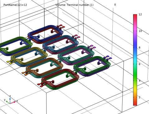
In the Settings window for Volume, click Replace Expression in the upper-right corner of the Expression section. From the menu, choose Component 1 (comp1) > Magnetic Fields, Currents Only > Conductors > mfco.TerminalNumber - Terminal number - 1.
3
Locate the Coloring and Style section. From the Color table list, choose Cyclic.
4
In the Terminal Number toolbar, click  Plot.
Add Study
1
In the Home toolbar, click  Add Study to open the Add Study window.
2
Go to the Add Study window.
3
Find the Studies subsection. In the Select Study tree, select Preset Studies for Selected Physics Interfaces > Frequency Domain Source Sweep with Initialization.
4
Click the Add Study button in the window toolbar.
5
In the Home toolbar, click  Add Study to close the Add Study window.
Study 2
Step 2: Frequency Domain Source Sweep
1
In the Settings window for Frequency Domain Source Sweep, locate the Study Settings section.
2
In the Frequencies text field, type 200[kHz].
3
In the Study toolbar, click  Compute.
Results
Magnetic Flux Density (mfco)
Right-click Results > Magnetic Flux Density (mfco) and choose Delete.
Magnetic Flux Density Norm (AC)
1
In the Model Builder window, right-click Magnetic Flux Density Norm (DC) and choose Duplicate.
2
In the Settings window for 3D Plot Group, type Magnetic Flux Density Norm (AC) in the Label text field.
3
Locate the Data section. From the Dataset list, choose Study 2/Solution 3 (sol3).
4
From the Parameter value (PortName) list, choose 8.
5
In the Magnetic Flux Density Norm (AC) toolbar, click  Plot.
Resistance (DC) (dset3, mfco)
1
In the Model Builder window, expand the Results > Lumped Parameters (dset3, mfco) node, then click Resistance (DC) (dset3, mfco).
2
In the Resistance (DC) (dset3, mfco) toolbar, click  Evaluate.
Resistance (AC) (dset3, mfco)
1
In the Model Builder window, click Resistance (AC) (dset3, mfco).
2
In the Resistance (AC) (dset3, mfco) toolbar, click  Evaluate.
Inductance (AC) (dset3, mfco)
1
In the Model Builder window, expand the Inductance (AC) (dset3, mfco) node, then click Inductance (AC) (dset3, mfco).
2
In the Settings window for Global Matrix Evaluation, locate the Data Series Operation section.
3
From the Parameter (freq) list, choose Sum.
4
In the Inductance (AC) (dset3, mfco) toolbar, click  Evaluate.
Impedance (dset3, mfco)
1
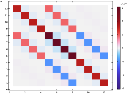
In the Model Builder window, under Results > Lumped Parameters (dset3, mfco) click Impedance (dset3, mfco).
2
In the Impedance (dset3, mfco) toolbar, click  Evaluate.
Inductance Matrix (AC)
1
In the Model Builder window, right-click Inductance Matrix (DC) and choose Duplicate.
2
In the Settings window for 2D Plot Group, type Inductance Matrix (AC) in the Label text field.
Table Surface 1
1
In the Model Builder window, expand the Inductance Matrix (AC) node, then click Table Surface 1.
2
In the Settings window for Table Surface, locate the Data section.
3
From the Evaluation group list, choose Inductance (AC) (dset3, mfco).
4
From the Data format list, choose Cells.
5
In the Inductance Matrix (AC) toolbar, click  Plot.