|
|
|
|
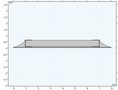
35 μm
|
|||
|
25 μm
|
|||
|
105 μm
|
|
1
|
|
2
|
In the Select Physics tree, select Structural Mechanics>Thermal–Structure Interaction>Thermal Stress, Solid.
|
|
3
|
Click Add.
|
|
4
|
Click
|
|
5
|
|
6
|
Click
|
|
1
|
|
2
|
|
1
|
|
2
|
|
3
|
|
1
|
|
2
|
|
3
|
|
4
|
|
5
|
|
1
|
|
2
|
|
3
|
|
4
|
|
5
|
|
6
|
|
1
|
|
2
|
|
3
|
|
4
|
|
5
|
|
6
|
|
7
|
|
1
|
|
2
|
|
3
|
|
4
|
|
5
|
|
6
|
|
1
|
|
2
|
|
3
|
|
1
|
|
2
|
|
3
|
|
4
|
|
5
|
|
6
|
|
1
|
|
2
|
|
3
|
|
4
|
|
5
|
|
6
|
|
7
|
|
8
|
|
1
|
|
2
|
|
3
|
|
4
|
|
5
|
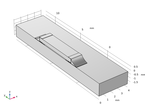
Select the object r3 only.
|
|
6
|
|
1
|
|
2
|
Select the object dif1 only.
|
|
3
|
|
4
|
|
5
|
|
6
|
|
7
|
|
1
|
|
2
|
|
3
|
|
4
|
|
5
|
|
6
|
|
7
|
|
1
|
|
2
|
On the object dif1, select Point 12 only.
|
|
3
|
|
4
|
|
5
|
On the object mir1, select Point 12 only.
|
|
6
|
|
1
|
|
2
|
Click in the Graphics window and then press Ctrl+A to select all objects.
|
|
3
|
|
1
|
|
2
|
Select the object csol2 only.
|
|
1
|
|
2
|
On the object uni1, select Domains 2, 5, and 7 only.
|
|
3
|
|
4
|
|
5
|
On the object uni1, select Boundaries 4, 11, and 30 only.
|
|
6
|
|
1
|
|
2
|
On the object pard1, select Domains 4 and 10 only.
|
|
3
|
|
4
|
|
5
|
On the object pard1, select Points 4–7, 22, 23, 25, and 26 only.
|
|
6
|
|
1
|
|
1
|
In the Model Builder window, under Component 1 (comp1)>Geometry 1 right-click Work Plane 1 (wp1) and choose Extrude.
|
|
2
|
Select the object wp1 only.
|
|
3
|
|
5
|
|
1
|
|
2
|
|
3
|
|
4
|
|
5
|
|
6
|
|
7
|
|
8
|
|
9
|
|
1
|
|
2
|
|
3
|
|
4
|
|
1
|
|
2
|
On the object fin, select Boundaries 17, 22, 25, 41, 59, 60, and 62 only.
|
|
3
|
|
1
|
|
2
|
|
3
|
|
4
|
|
5
|
In the tree, select Built-in>Alumina.
|
|
6
|
|
7
|
In the tree, select Built-in>Copper.
|
|
8
|
|
9
|
|
10
|
|
11
|
|
12
|
|
13
|
In the tree, select Built-in>Air.
|
|
14
|
|
15
|
|
1
|
|
2
|
|
3
|
|
4
|
|
1
|
|
1
|
|
1
|
|
1
|
|
1
|
|
1
|
|
2
|
|
3
|
|
4
|
|
5
|
|
1
|
|
1
|
|
2
|
|
3
|
|
1
|
|
1
|
|
3
|
|
4
|
|
1
|
|
3
|
|
4
|
|
1
|
|
3
|
|
4
|
|
1
|
|
1
|
|
3
|
|
4
|
|
5
|
|
1
|
|
3
|
|
4
|
|
5
|
|
6
|
|
1
|
|
2
|
|
3
|
|
1
|
|
1
|
|
3
|
|
4
|
Click the Custom button.
|
|
5
|
|
6
|
|
1
|
|
1
|
|
2
|
|
3
|
Click the Custom button.
|
|
4
|
|
5
|
|
1
|
|
2
|
|
3
|
|
5
|
|
6
|
|
7
|
|
1
|
|
2
|
|
3
|
|
4
|
|
1
|
|
2
|
|
3
|
In the Model Builder window, expand the Study 1>Solver Configurations>Solution 1 (sol1)>Stationary Solver 1 node, then click Segregated 1.
|
|
4
|
|
5
|
|
6
|
In the Model Builder window, expand the Study 1>Solver Configurations>Solution 1 (sol1)>Stationary Solver 1>Segregated 1 node, then click Temperature.
|
|
7
|
|
8
|
|
9
|
|
10
|
In the Model Builder window, under Study 1>Solver Configurations>Solution 1 (sol1)>Stationary Solver 1>Segregated 1 click Solid Mechanics.
|
|
11
|
|
12
|
|
13
|
|
14
|
|
1
|
|
2
|
|
3
|
|
1
|
|
2
|
|
3
|
|
4
|
|
1
|
|
2
|
|
1
|
|
2
|
|
3
|
|
4
|
|
1
|
|
2
|
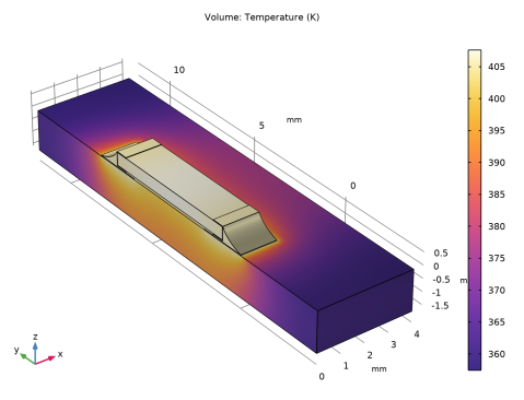
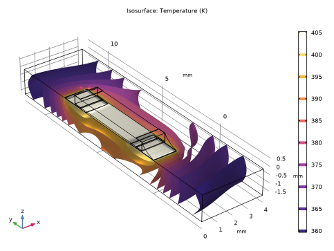
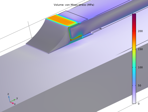
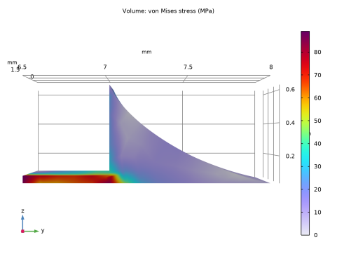
In the Settings window for Volume, click Replace Expression in the upper-right corner of the Expression section. From the menu, choose Component 1 (comp1)>Solid Mechanics>Stress>solid.misesGp - von Mises stress - N/m².
|
|
3
|
|
4
|
|
5
|
|
6
|
Click OK.
|
|
1
|
|
3
|
|
4
|
|
1
|
|
2
|