|
|
|


|
1
|
|
2
|
|
3
|
Click Add.
|
|
4
|
Click
|
|
5
|
|
6
|
Click
|
|
1
|
|
2
|
|
3
|
|
4
|
Browse to the model’s Application Libraries folder and double-click the file tapered_waveguide_parameters.txt.
|
|
1
|
|
2
|
In the Part Libraries window, select Wave Optics Module>Slab Waveguides>slab_waveguide_taper in the tree.
|
|
3
|
|
1
|
In the Model Builder window, under Component 1 (comp1)>Geometry 1 click Slab Waveguide Taper 1 (pi1).
|
|
2
|
|
3
|
|
4
|
|
5
|
|
6
|
|
7
|
Click OK.
|
|
8
|
|
9
|
|
10
|
|
11
|
Click OK.
|
|
12
|
|
14
|
|
15
|
|
1
|
|
2
|
|
3
|
In the Part Libraries window, select Wave Optics Module>Slab Waveguides>slab_waveguide_straight in the tree.
|
|
4
|
|
1
|
In the Model Builder window, under Component 1 (comp1)>Geometry 1 click Slab Waveguide Straight 1 (pi2).
|
|
2
|
|
3
|
|
4
|
Locate the Position and Orientation of Output section. In the x-displacement text field, type -lam0.
|
|
5
|
|
6
|
|
8
|
|
9
|
In the New Cumulative Selection dialog box, type Straight Waveguide Transverse Perimeter in the Name text field.
|
|
10
|
Click OK.
|
|
11
|
|
13
|
|
14
|
|
1
|
|
2
|
|
3
|
Locate the Position and Orientation of Output section. In the x-displacement text field, type -2*lam0.
|
|
4
|
|
5
|
|
6
|
Click OK.
|
|
7
|
|
9
|
|
10
|
|
11
|
|
1
|
In the Model Builder window, under Component 1 (comp1)>Geometry 1 right-click Input Waveguide (pi2) and choose Duplicate.
|
|
2
|
|
3
|
|
4
|
Locate the Position and Orientation of Output section. In the x-displacement text field, type d_taper.
|
|
5
|
|
6
|
|
7
|
|
1
|
In the Model Builder window, under Component 1 (comp1)>Geometry 1 right-click Input PML (pi3) and choose Duplicate.
|
|
2
|
|
3
|
|
4
|
Locate the Position and Orientation of Output section. In the x-displacement text field, type d_taper+lam0.
|
|
5
|
|
6
|
|
7
|
|
1
|
In the Model Builder window, under Component 1 (comp1) right-click Materials and choose Blank Material.
|
|
2
|
|
3
|
|
1
|
|
2
|
|
3
|
|
4
|
|
1
|
|
2
|
|
3
|
|
4
|
|
5
|
In the Typical wavelength text field, type 2*pi/kx. The variable kx will be highlighted in orange to warn that it has not been defined yet.
|
|
1
|
In the Model Builder window, under Component 1 (comp1) click Electromagnetic Waves, Beam Envelopes (ewbe).
|
|
2
|
|
3
|
|
4
|
|
5
|
|
6
|
In the φ1 text field, type phi. The variable phi will also be displayed in orange, as it has not yet been defined.
|
|
7
|
|
1
|
|
2
|
|
3
|
|
4
|
|
5
|
|
6
|
|
7
|
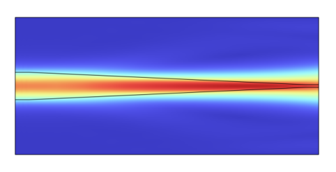
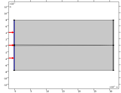
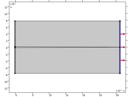
Click Toggle Power Flow Direction to make the arrows in the Graphics window point in the positive x direction (meaning that the power will flow into the tapered waveguide).
|
|
1
|
|
2
|
|
3
|
|
4
|
|
5
|
|
6
|
|
7
|
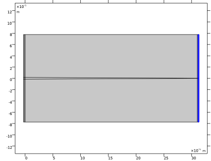
Click Toggle Power Flow Direction to make the arrows in the Graphics window point in the positive x direction (meaning that the power will flow out of the waveguide and into the backing PML).
|
|
1
|
In the Model Builder window, under Component 1 (comp1) right-click Definitions and choose Variables.
|
|
2
|
|
3
|
|
4
|
|
5
|
|
6
|
Locate the Variables section. In the table, enter the following settings:
|
|
1
|
|
2
|
|
3
|
Locate the Geometric Entity Selection section. From the Selection list, choose All (Input Waveguide).
 |
|
4
|
Locate the Variables section. In the table, enter the following settings:
|
|
1
|
|
2
|
|
3
|
Locate the Geometric Entity Selection section. From the Selection list, choose All (Tapered Waveguide).
 |
|
4
|
Locate the Variables section. In the table, enter the following settings:
|
|
1
|
|
2
|
|
3
|
Locate the Geometric Entity Selection section. From the Selection list, choose All (Output Waveguide).
 |
|
4
|
Locate the Variables section. In the table, enter the following settings:
|
|
1
|
|
2
|
|
3
|
|
4
|
Locate the Variables section. In the table, enter the following settings:
|
|
1
|
|
2
|
|
3
|
|
1
|
|
2
|
|
3
|
|
4
|
|
1
|
|
2
|
|
3
|
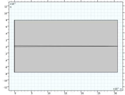
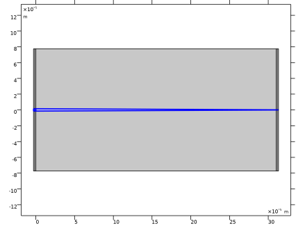
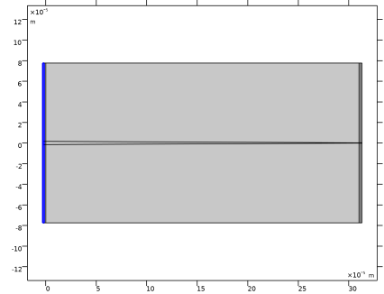
From the Selection list, choose Port 1 core (Input PML). This is the leftmost boundary adjacent to the core domain.
 |
|
4
|
|
1
|
|
2
|
|
3
|
Select the Adjust edge mesh check box. This makes sure the PML mesh, especially on the input side, is not skewed.
|
|
1
|
|
2
|
|
3
|
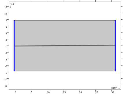
From the Selection list, choose Straight Waveguide Transverse Perimeter. The selected entities are the top and bottom boundaries adjacent to the straight (non-tapered) waveguide domains.
 |
|
4
|
|
1
|
|
2
|
|
3
|
|
4
|
|
5
|
|
1
|
|
2
|
|
3
|
Click
|
|
5
|
Click
|
|
6
|
|
7
|
|
8
|
|
9
|
|
10
|
Click Replace.
|
|
1
|
|
2
|
|
3
|
|
4
|
|
1
|
|
2
|
|
3
|
|
1
|
In the Model Builder window, under Study 1 right-click Step 1: Wavelength Domain and choose Move Down. Repeat this operation once more. You can also move the Step1: Wavelength Domain node down to the last position in the list by selecting it and clicking Ctrl+Down twice.
|
|
2
|
|
3
|
|
4
|
|
1
|
|
2
|
|
3
|
|
4
|
|
5
|
|
1
|
|
2
|
|
3
|
|
4
|
|
1
|
|
2
|
|
3
|
|
4
|
|
5
|
|
6
|
|
7
|
Click
|
|
1
|
|
1
|
In the Model Builder window, under Results click Reflectance, Transmittance, and Absorptance (ewbe).
|
|
2
|
|
3
|
|
4
|
|
5
|
|
1
|
|
2
|
|
4
|
Click
|
|
6
|
Click
|
|
7
|
|
1
|
|
2
|
|
3
|
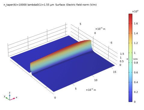
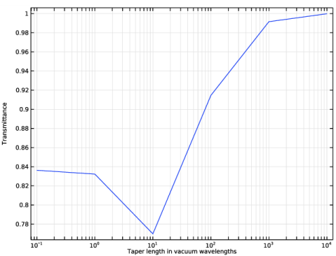
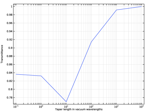
From the Parameter selection (n_taper) list, choose First to just plot one of the curves since they are all the same.
|
|
1
|
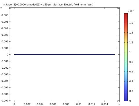
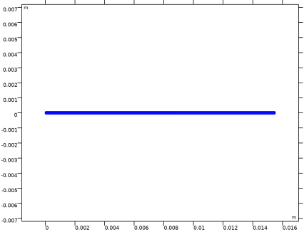
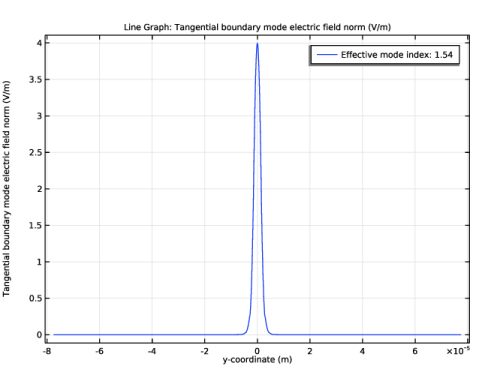
In the Model Builder window, expand the Electric Mode Field, Port 1 (ewbe) node, then click Line Graph 1.
|
|
2
|
|
3
|
|
4
|
|
5
|
|
1
|
|
2
|
|
3
|
|
1
|
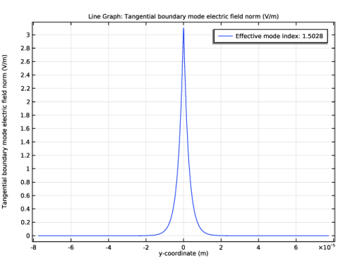
In the Model Builder window, expand the Electric Mode Field, Port 2 (ewbe) node, then click Line Graph 1.
|
|
2
|
|
3
|
|
4
|
|
5
|