PDF

Photonic Crystal
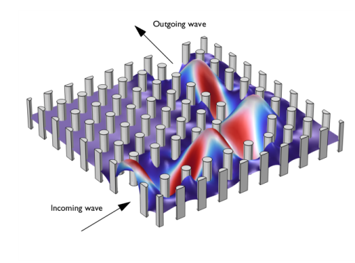
Photonic crystal devices are periodic structures of alternating layers of materials with different refractive indices. Waveguides that are confined inside of a photonic crystal can have very sharp low-loss bends, which may enable an increase in integration density of several orders of magnitude.
Introduction
This application describes the wave propagation in a photonic crystal that consists of GaAs pillars placed equidistant from each other. The distance between the pillars prevents light of certain wavelengths to propagate into the crystal structure. Depending on the distance between the pillars, waves within a specific frequency range are reflected instead of propagating through the crystal. This frequency range is called the photonic band gap (Ref. 1). By removing some of the GaAs pillars in the crystal structure you can create a guide for the frequencies within the band gap. Light can then propagate along the outlined guide geometry.
Model Definition
The geometry is a square of air with an array of circular pillars of GaAs as described above. Some pillars are removed to make a waveguide with a 90° bend.
The objective of the application is to study TE waves propagating through the crystal. To model these, use a scalar equation for the transverse electric field component Ez,
where n is the refractive index and k0 is the free-space wave number.
Because there are no physical boundaries, you can use the scattering boundary condition at all boundaries. Set the amplitude Ez to 1 on the boundary of the incoming wave.
Results and Discussion
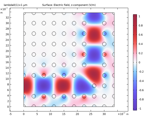
Figure 1 contains a plot of the z-component of the electric field. It clearly shows the propagation of the wave through the guide.
Figure 1: The z-component of the electric field showing how the wave propagates along the path defined by the pillars.
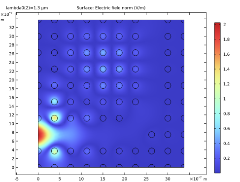
If the angular frequency of the incoming wave is less than the cutoff frequency of the waveguide, the wave does not propagate through the outlined guide geometry. In Figure 2 the wavelength has been increased by a factor of 1.3.
Figure 2: A longer wavelength does not propagate through the guide. This plot shows the norm of the electric field.
Reference
1. J.D. Joannopoulos, R.D. Meade, and J.N. Winn, Photonic Crystals (Modeling the Flow of Light), Princeton University Press, 1995.
Application Library path: Wave_Optics_Module/Waveguides_and_Couplers/photonic_crystal
Modeling Instructions
From the File menu, choose New.
New
In the New window, click  Model Wizard.
Model Wizard
1
In the Model Wizard window, click  2D.
2
In the Select Physics tree, select Optics>Wave Optics>Electromagnetic Waves, Frequency Domain (ewfd).
3
Click Add.
4
Click  Study.
5
In the Select Study tree, select Preset Studies for Selected Physics Interfaces>Wavelength Domain.
6
Geometry 1
Import 1 (imp1)
1
In the Home toolbar, click  Import.
2
In the Settings window for Import, locate the Import section.
3
Click  Browse.
4
5
Click  Import.
6
Click the  Zoom Extents button in the Graphics toolbar.
Materials
The refractive index of GaAs depends on the frequency. The material is added from the Optical Material Database.
Add Material
1
In the Home toolbar, click  Add Material to open the Add Material window.
2
Go to the Add Material window.
3
In the tree, select Optical>Inorganic Materials>As - Arsenides>Experimental data>GaAs (Gallium arsenide) (Skauli et al. 2003: n 0.97-17 um).
4
Click Add to Component in the window toolbar.
5
In the Home toolbar, click  Add Material to close the Add Material window.
Materials
GaAs (Gallium arsenide) (Skauli et al. 2003: n 0.97-17 um) (mat1)
Select Domains 1 and 3–86 only. This is most easily done by removing Domain 2 from the list once you have selected all domains.
Air
1
In the Model Builder window, right-click Materials and choose Blank Material.
2
In the Settings window for Material, type Air in the Label text field.
3
4
Locate the Material Contents section. In the table, enter the following settings:
Electromagnetic Waves, Frequency Domain (ewfd)
1
In the Model Builder window, under Component 1 (comp1) click Electromagnetic Waves, Frequency Domain (ewfd).
2
In the Settings window for Electromagnetic Waves, Frequency Domain, locate the Components section.
3
From the Electric field components solved for list, choose Out-of-plane vector, as only the out-of-plane component will be solved for.
Scattering Boundary Condition 1
1
In the Physics toolbar, click  Boundaries and choose Scattering Boundary Condition.
2
In the Settings window for Scattering Boundary Condition, locate the Boundary Selection section.
3
From the Selection list, choose All boundaries.
Scattering Boundary Condition 2
1
In the Physics toolbar, click  Boundaries and choose Scattering Boundary Condition.
2
3
In the Settings window for Scattering Boundary Condition, locate the Scattering Boundary Condition section.
4
From the Incident field list, choose Wave given by E field.
5
Specify the E0 vector as
Study 1
Step 1: Wavelength Domain
1
In the Model Builder window, under Study 1 click Step 1: Wavelength Domain.
2
In the Settings window for Wavelength Domain, locate the Study Settings section.
3
In the Wavelengths text field, type 1[um] 1.3[um].
This will get you one solution for a free space wavelength of 1 μm, and one for a free space wavelength of 1.3 μm.
4
In the Home toolbar, click  Compute.
Results
Electric Field (ewfd)
The default plot shows the distribution of the electric field norm for the lowest of the frequencies. Because this is below the cutoff frequency of the waveguide, the wave does not propagate through the outlined guide geometry.
1
In the Settings window for 2D Plot Group, locate the Data section.
2
From the Parameter value (lambda0 (µm)) list, choose 1.
3
In the Electric Field (ewfd) toolbar, click  Plot.
300 THz, or a free space wavelength of 1 μm, is within the band gap. The wave propagates all the way through the geometry, losing only a little of its energy. Try visualizing the instantaneous value of the field.
Surface 1
1
In the Model Builder window, expand the Electric Field (ewfd) node, then click Surface 1.
2
In the Settings window for Surface, click Replace Expression in the upper-right corner of the Expression section. From the menu, choose Component 1 (comp1)>Electromagnetic Waves, Frequency Domain>Electric>Electric field - V/m>ewfd.Ez - Electric field, z-component.
3
Locate the Coloring and Style section. Click  Change Color Table.
4
In the Color Table dialog box, select Wave>WaveLight in the tree.
5
The WaveLight color table looks better if the range is symmetric around zero.
6
In the Settings window for Surface, locate the Coloring and Style section.
7
From the Scale list, choose Linear symmetric.
8
In the Electric Field (ewfd) toolbar, click  Plot.
Cut Line 2D 1
Finally, create a line plot comparing how the electric field magnitude falls off as the waves of the two frequencies under study enter the waveguide.
1
In the Results toolbar, click  Cut Line 2D.
2
In the Settings window for Cut Line 2D, locate the Line Data section.
3
In row Point 1, set Y to 0.75e-6.
4
In row Point 2, set X to 2.5e-6 and y to 0.75e-6.
5
1D Plot Group 2
1
In the Results toolbar, click  1D Plot Group.
2
In the Settings window for 1D Plot Group, locate the Data section.
3
From the Dataset list, choose Cut Line 2D 1.
Line Graph 1
1
Right-click 1D Plot Group 2 and choose Line Graph.
2
In the 1D Plot Group 2 toolbar, click  Plot.