PDF

Optical Yagi–Uda Antenna
Introduction
A Yagi–Uda antenna is a well-known antenna type in RF and microwave communication. The most common Yagi–Uda antenna consists of a feed element, a reflector, and an array of directors. The lengths and spacings of the elements are specifically designed to achieve high directivity.
By utilizing the strong plasmonic response of metallic nanostructures, the concept of antenna can be generalized to the optical regime. Optical antennas offer important functionalities such as the manipulation of light at the nanoscale.
This model demonstrates the modeling of an optical Yagi–Uda antenna made of aluminum nanorods using the boundary element method (BEM) in the Electromagnetic Waves, Boundary Elements interface of the Wave Optics Module.
Figure 1: An optical Yagi–Uda antenna made of aluminum nanorods.
Model Definition
The optical Yagi–Uda antenna is constituted of aluminum nanorods of radius 20 nm. The nanorods have hemispherical caps on both sides. The antenna is designed to operate at 570 nm wavelength, where aluminum has permittivity of 38 − 10.9j. Due to the finite loss of metal at optical frequency, the lengths and spacings of the elements are different from an RF Yagi–Uda antenna for which the electromagnetic loss is negligible. In this particular design as shown in Ref. 1, the length of the feed element is 160 nm. The lengths of the reflector and director are 200 nm and 144 nm, respectively. The spacing between the reflector and the feed is about 130 nm. The spacing between the feed and the first director, as well as the director array spacing, is about 140 nm.
An optical Yagi–Uda antenna usually is driven by a quantum emitter such as a quantum dot near the end of the feed element. In simulation, the quantum emitter can be approximated as a classical electrical point dipole. To implement the electrical point dipole drive, the scattered field formulation was used with the background field set as the dipole field. Assuming the dipole is located at (xp,yp,zp), the electric field at a point (x,y,z) in space is then given by the classical dipole field
(1),
where p = (px,py,pz) is the dipole moment, c is the speed of light, ε0 is the vacuum permittivity, ω is the angular frequency, R = (x − xp,y − yp,z − zp) is the distance vector from the dipole position to the field position in space, is the unit vector of R, and R is the norm of R. In this model, we only simulate an electric dipole located at (0,100 nm, 0) and oriented in the y direction, that is, p = (0,py,0). To avoid entering long expressions for each component of the background field, we define variables K = 1/(4πε0), F1 = ω2/(c2R), F2 = 1/R3+jω/(cR2), and F3 = exp(jωr/c) in the model.
Results and Discussion
In the finite element method (FEM) used in the Electromagnetic Waves, Frequency Domain interface, we can only evaluate field quantities within the finite simulation domain. The advantage of BEM is that field quantities can be evaluated everywhere, even if only boundaries are meshed. This is well suited for radiation problems. For example, in this model, the air domain surrounding the antenna will not be meshed. Nevertheless, the field evaluation can be done by using a Grid 3D dataset. We set the dataset range in the x, y, and z directions to 5000 nm to 5000 nm. The resolutions are set to 200 to ensure we can resolve the details of the field distribution. The plotted norm of the electric field is shown in Figure 2. This dataset covers a volume of ~20λ-by-~20λ-by-~20λ. It is generally not feasible to simulate such a large domain in FEM. Besides the Grid 3D dataset, other datasets such as Parameterized Surface and Parameterized Curve 3D can also be used to evaluate quantities of interest.
Furthermore, in order to obtain the far-field radiation characteristics of the antenna, a Far-Field Calculation node is applied on the boundaries of all antenna elements. This enables the evaluation of the far field quantities in postprocessing. The far-field radiation pattern shows a high directivity, which verifies the validity of the design.
Figure 2: Norm of the electric field around the optical Yagi–Uda antenna. Using the Grid 3D dataset, we can evaluate the field quantities at arbitrary locations.
Figure 3: Far-field radiation pattern of the optical Yagi–Uda antenna, showing a high directivity.
Notes About the COMSOL Implementation
This model uses the Electromagnetic Waves, Boundary Elements interface to demonstrate its functionalities. In principle, the Electromagnetic Waves, Frequency Domain interface can be used to model the same structure and achieve the same results. Both BEM and FEM solve the full Maxwell equations but FEM requires a finite simulation domain with volumetric meshing while BEM can model infinite domain and only require boundary meshing. Although the degrees of freedom in a BEM model are generally fewer compared to FEM, the memory and computation time requirements are not necessarily smaller. Therefore, one method could be more efficient than the other, depending on the type of problem to be solved.
When using the Electromagnetic Waves, Boundary Elements interface to model dielectrics scatterers, additional Wave Equation, Electric nodes must be added and applied to all finite domains representing the scatterers. The first Wave Equation, Electric node should only contain the finite void when using the scattered field formulation. The best practice is to apply one separate Wave Equation, Electric node to each enclosed domain individually. In this model, however, we only apply one Wave Equation, Electric node to all the dielectric domains since there is only one material involved.
Reference
1. T.H. Taminiau, F.D. Stefani, and N.F. van Hulst, “Enhanced directional excitation and emission of single emitters by a nano-optical Yagi–Uda antenna,” Optics Express, vol. 165, no. 14, pp. 10858–10866, 2008.
Application Library path: Wave_Optics_Module/Optical_Scattering/optical_yagi_uda_antenna
Modeling Instructions
From the File menu, choose New.
New
In the New window, click  Model Wizard.
Model Wizard
1
In the Model Wizard window, click  3D.
2
In the Select Physics tree, select Optics>Wave Optics>Electromagnetic Waves, Boundary Elements (ebem).
3
Click Add.
4
Click  Study.
5
In the Select Study tree, select Preset Studies for Selected Physics Interfaces>Wavelength Domain.
6
Geometry 1
1
In the Model Builder window, under Component 1 (comp1) click Geometry 1.
2
In the Settings window for Geometry, locate the Units section.
3
From the Length unit list, choose nm.
Global Definitions
Parameters 1
1
In the Model Builder window, under Global Definitions click Parameters 1.
2
In the Settings window for Parameters, locate the Parameters section.
3
Definitions
Variables 1
1
In the Model Builder window, under Component 1 (comp1) right-click Definitions and choose Variables.
2
In the Settings window for Variables, locate the Variables section.
3
Here we define the distance from the point dipole position to a point in space at (x,y,z) as well as the components of the unit vector connecting them. The variables K, F1, F2, and F3 are defined for convenience to avoid typing long and repeated expressions in the background field.
Geometry 1
Cylinder 1 (cyl1)
1
In the Geometry toolbar, click  Cylinder.
2
In the Settings window for Cylinder, locate the Size and Shape section.
3
In the Radius text field, type r.
4
In the Height text field, type L_r-2*r.
5
Locate the Position section. In the x text field, type -a_r.
6
In the y text field, type -(L_r-2*r)/2.
7
Locate the Axis section. From the Axis type list, choose y-axis.
Cylinder 2 (cyl2)
1
Right-click Cylinder 1 (cyl1) and choose Duplicate.
2
In the Settings window for Cylinder, locate the Size and Shape section.
3
In the Height text field, type L_f-2*r.
4
Locate the Position section. In the x text field, type 0.
5
In the y text field, type -(L_f-2*r)/2.
Cylinder 3 (cyl3)
1
Right-click Cylinder 2 (cyl2) and choose Duplicate.
2
In the Settings window for Cylinder, locate the Size and Shape section.
3
In the Height text field, type L_d-2*r.
4
Locate the Position section. In the y text field, type -(L_d-2*r)/2.
5
In the x text field, type a_d.
Sphere 1 (sph1)
1
In the Geometry toolbar, click  Sphere.
2
In the Settings window for Sphere, locate the Size section.
3
In the Radius text field, type r.
4
Locate the Position section. In the y text field, type L_f/2-r.
Sphere 2 (sph2)
1
Right-click Sphere 1 (sph1) and choose Duplicate.
2
In the Settings window for Sphere, locate the Position section.
3
In the y text field, type -L_f/2+r.
Sphere 3 (sph3)
1
Right-click Sphere 2 (sph2) and choose Duplicate.
2
In the Settings window for Sphere, locate the Position section.
3
In the x text field, type -a_r.
4
In the y text field, type -L_r/2+r.
Sphere 4 (sph4)
1
Right-click Sphere 3 (sph3) and choose Duplicate.
2
In the Settings window for Sphere, locate the Position section.
3
In the y text field, type L_r/2-r.
Sphere 5 (sph5)
1
Right-click Sphere 4 (sph4) and choose Duplicate.
2
In the Settings window for Sphere, locate the Position section.
3
In the x text field, type a_d.
4
In the y text field, type L_d/2-r.
Sphere 6 (sph6)
1
Right-click Sphere 5 (sph5) and choose Duplicate.
2
In the Settings window for Sphere, locate the Position section.
3
In the y text field, type -L_d/2+r.
Array 1 (arr1)
1
In the Geometry toolbar, click  Transforms and choose Array.
2
Select the objects cyl3, sph5, and sph6 only.
3
In the Settings window for Array, locate the Size section.
4
In the x size text field, type 3.
5
Locate the Displacement section. In the x text field, type a_d.
Materials
Air
1
In the Model Builder window, under Component 1 (comp1) right-click Materials and choose Blank Material.
2
In the Settings window for Material, type Air in the Label text field.
3
Locate the Geometric Entity Selection section. From the Selection list, choose All voids.
4
Locate the Material Contents section. In the table, enter the following settings:
Al
1
Right-click Materials and choose Blank Material.
2
In the Settings window for Material, type Al in the Label text field.
3
Click the  Select All button in the Graphics toolbar.
4
Locate the Material Contents section. In the table, enter the following settings:
Next, change the Formulation to Scattered field and set up the background field, which is the field created by an electrical point dipole as given by .
Electromagnetic Waves, Boundary Elements (ebem)
1
In the Model Builder window, under Component 1 (comp1) click Electromagnetic Waves, Boundary Elements (ebem).
2
In the Settings window for Electromagnetic Waves, Boundary Elements, locate the Formulation section.
3
From the list, choose Scattered field.
4
Specify the Eb vector as
Wave Equation, Electric 2
1
In the Physics toolbar, click  Domains and choose Wave Equation, Electric.
A Wave Equation, Electric node is added and applied to the antenna domains. This node includes all the finite domains of the same material. The first Wave Equation, Electric node should only contains the infinite void when using the scattered field formulation.
2
Click the  Select All button in the Graphics toolbar.
Far-Field Calculation 1
1
In the Physics toolbar, click  Boundaries and choose Far-Field Calculation.
2
Click the  Select All button in the Graphics toolbar.
A Far-Field Calculation is added so later in the postprocessing we can evaluate the far-field radiation pattern.
Study 1
Step 1: Wavelength Domain
1
In the Model Builder window, under Study 1 click Step 1: Wavelength Domain.
2
In the Settings window for Wavelength Domain, locate the Study Settings section.
3
In the Wavelengths text field, type lda0.
4
In the Home toolbar, click  Compute.
Results
Grid 3D 1
1
In the Model Builder window, expand the Results>Datasets node, then click Grid 3D 1.
2
In the Settings window for Grid 3D, locate the Parameter Bounds section.
3
Find the First parameter subsection. In the Minimum text field, type -5000.
4
In the Maximum text field, type 5000.
5
Find the Second parameter subsection. In the Minimum text field, type -5000.
6
In the Maximum text field, type 5000.
7
Find the Third parameter subsection. In the Minimum text field, type -5000.
8
In the Maximum text field, type 5000.
9
Click to expand the Grid section. In the x resolution text field, type 200.
10
In the y resolution text field, type 200.
11
In the z resolution text field, type 200.
In FEM, we can only visualize the physical quantities such as the electric field within the simulation domain. However, in BEM, we are free to visualize them everywhere by using a Grid 3D dataset, which is added by default.
Electric Field, Domains (ebem)
1
In the Model Builder window, under Results click Electric Field, Domains (ebem).
2
In the Settings window for 3D Plot Group, click to expand the Title section.
3
From the Title type list, choose None.
Multislice 1
1
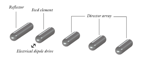
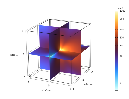
In the Model Builder window, expand the Electric Field, Domains (ebem) node, then click Multislice 1.
2
In the Settings window for Multislice, click to expand the Range section.
3
Select the Manual color range check box.
4
In the Minimum text field, type 0.
5
In the Maximum text field, type 1e8.
6
Locate the Coloring and Style section. From the Scale list, choose Logarithmic.
7
Click  Change Color Table.
8
In the Color Table dialog box, select Thermal>ThermalWave in the tree.
9
First, plot the norm of the electric field around the Yagi–Uda antenna. To enhance the visualization, use a logarithmic scale. Next, plot the far-field radiation pattern.
3D Plot Group 4
1
In the Home toolbar, click  Add Plot Group and choose 3D Plot Group.
2
In the Settings window for 3D Plot Group, click to expand the Title section.
3
From the Title type list, choose None.
Radiation Pattern 1
1
In the 3D Plot Group 4 toolbar, click  More Plots and choose Radiation Pattern.
2
In the Settings window for Radiation Pattern, locate the Expression section.
3
In the Expression text field, type ebem.normEfar^2.
4
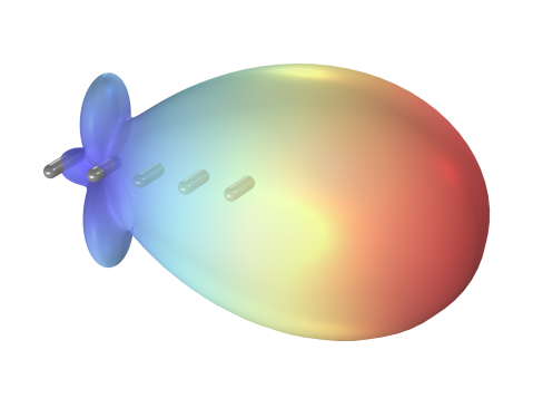
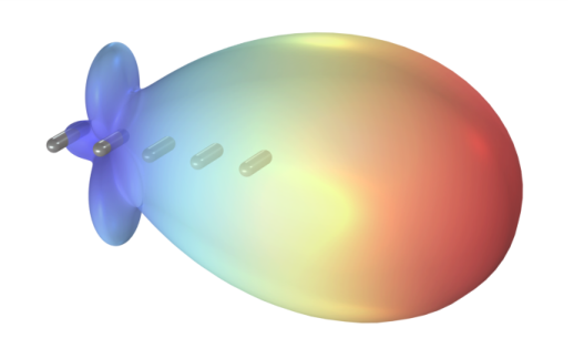
Locate the Evaluation section. Find the Angles subsection. In the Number of elevation angles text field, type 100.
5
In the Number of azimuth angles text field, type 100.
6
Locate the Coloring and Style section. Clear the Color legend check box.
Transparency 1
1
Right-click Radiation Pattern 1 and choose Transparency.
2
In the Settings window for Transparency, locate the Transparency section.
3
Set the Transparency value to 0.35.
Surface 1
In the Model Builder window, right-click 3D Plot Group 4 and choose Surface.
Material Appearance 1
1
In the Model Builder window, right-click Surface 1 and choose Material Appearance.
2
Click the  Show Axis Orientation button in the Graphics toolbar.
3
Click the  Show Grid button in the Graphics toolbar.
4
In the Settings window for Material Appearance, locate the Appearance section.
5
From the Appearance list, choose Custom.
6
From the Material type list, choose Aluminum.
7
Click Customize.
8
Set the Reflectance at normal incidence value to 0.45.
9
Set the Surface roughness value to 0.4.
10
Set the Anisotropy value to 0.35.
The visualization is enhanced by adding Material Appearance on the antenna surface.