PDF

Nanorods
Introduction
A Gaussian electromagnetic wave is incident on a dense array of very thin wires (or rods). The distance between the rods and, thus, also the rod diameter is much smaller than the wavelength. Under these circumstances, the rod array does not function as a diffraction grating (see the Plasmonic Wire Grating model). Instead, the rod array behaves as if it was a continuous metal sheet for light polarized along the rods, whereas for light polarized perpendicular to the rods, the array is almost transparent to the electromagnetic wave. However, for the latter case dipole coupling between the rods occurs, thereby coupling electromagnetic excitation between the rods also outside of the illuminated region.
Model Definition
Figure 1 shows the array of rods and the incident Gaussian beam. The beam propagates in negative y direction. The wavelength is 750 nm and the spot radius of the beam equals the wavelength. For a more detailed discussion about Gaussian beams, see the model Second Harmonic Generation of a Gaussian Beam.
For the tightly focused beam that is used in this example, a plane-wave expansion that approximates the well-known paraxial approximation of a Gaussian beam is used. The advantage of using the plane-wave expansion is that it is a true solution to the Helmholtz equation, as each plane wave is a solution to Helmholtz equation. Mathematically, what happens here is that the 2D Gaussian beam expression (the paraxial approximation)
(1)
is approximated by a plane wave expansion
(2),
where each wave vector kj points in different directions for each value of the index j and ajk is the amplitude that has a different value for each wave vector and also for each of the two possible polarization directions per wave vector, . So for a tightly focused beam, the paraxial approximation in Equation 1 does not approximate the Helmholtz equation well, whereas Equation 2 is a true solution to Helmholtz equation.
Figure 1: The modeled array of nanorods and the incident Gaussian beam. The model solves for the electric field in a 2D plane. Thus, the beam and rod properties are constant in the out-of-plane dimension.
The rods radius is 20 nm and the separation between the rods is 150 nm. Figure 1 shows that half of the beam illuminates the first part of the array of rods. Thus, most of the 40 rods in the model have a very low illumination.
The rods are metallic, with a dispersion formula for the relative permittivity given by
where the angular frequency is defined by
and ωp is the plasma frequency. The plasma frequency is set to , resulting in a negative relative permittivity similar to that of gold.
Results and Discussion
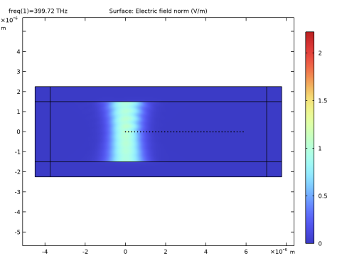
Figure 2 shows the norm of the electric field for the Gaussian beam. In this configuration, the light beam is polarized in the x direction, that is, in the direction of the grating vector. As seen from the surface plot, the nanorod array illuminates half of the Gaussian light beam. However, for this polarization there is no noticeable reflection nor diffraction from the nanorod array.
Figure 2: Surface plot of the electric field norm. The electric field of the Gaussian light beam is polarized in the x direction (along the grating vector).
Figure 3 shows a zoom-in of the leftmost part of the nanorod array and the center of the light beam. The plot shows that there is a dipolar coupling between the rods. Figure 4 shows that the coupling between the nanorods extends much longer than the intensity distribution of the exciting Gaussian light beam.
Figure 3: Zoom-in on the center of the Gaussian beam and the leftmost nanorods. As for Figure 2, the polarization of the beam is in the x direction.
Figure 4: Line plot of the x component of the electric field (blue line) and the Gaussian beam background field (green line). The beam is polarized in the x direction.
When the light beam is polarized along the rods, that is, in the z direction (the out-of-plane direction), the interaction between the beam and the nanorod array is much stronger. As a comparison to Figure 3, Figure 5 shows a zoom-in of the center of the Gaussian beam and the leftmost nanorods. When the beam is polarized in the out-of-plane direction, the nanorod array appears for the beam almost as an opaque metal sheet. Thus, the beam is reflected and there is strong edge diffraction.
Figure 5: Zoom-in of the electric field norm for the center of the Gaussian beam and the leftmost nanorods. The Gaussian light beam is polarized along the rods (out-of-plane in the z direction).
The effects of reflection and edge diffraction is very obvious from Figure 6. Above the array there is a standing wave, formed by the incident beam and the beam reflected from the array, and below the array edge diffraction is evident.
Figure 6: Surface plot of the full Gaussian beam and all the nanorods. The beam is polarized in the out-of-plane (z) direction.
Notes About the COMSOL Implementation
This application implementation demonstrates the use of perfectly matched layers for absorbing a propagating wave. Furthermore, when defining the relative permittivity, the Drude–Lorentz dispersion model is used. This setting is found in the wave equation feature.
Application Library path: Wave_Optics_Module/Optical_Scattering/nanorods
Modeling Instructions
From the File menu, choose New.
New
In the New window, click  Model Wizard.
Model Wizard
1
In the Model Wizard window, click  2D.
2
In the Select Physics tree, select Optics>Wave Optics>Electromagnetic Waves, Frequency Domain (ewfd).
3
Click Add.
4
Click  Study.
5
In the Select Study tree, select General Studies>Frequency Domain.
6
Global Definitions
Add parameters for the Gaussian light beam, the geometry, and the materials.
Parameters 1
1
In the Model Builder window, under Global Definitions click Parameters 1.
2
In the Settings window for Parameters, locate the Parameters section.
3
Geometry 1
Rectangle 1 (r1)
1
In the Geometry toolbar, click  Rectangle.
2
In the Settings window for Rectangle, locate the Size and Shape section.
3
In the Width text field, type w_air+2*d_PML.
4
In the Height text field, type h_air+2*d_PML.
5
Locate the Position section. In the x text field, type -w_air_left-d_PML.
6
In the y text field, type -h_air/2-d_PML.
Now create layers surrounding the rectangle for the perfectly matched layers (PMLs).
7
Click to expand the Layers section. In the table, enter the following settings:
8
Select the Layers to the left check box.
9
Select the Layers to the right check box.
10
Select the Layers on top check box.
The check box for the bottom layer is selected by default.
Circle 1 (c1)
Create the nanorods by first defining a circle, and then create a linear array of those circles.
1
In the Geometry toolbar, click  Circle.
2
In the Settings window for Circle, locate the Size and Shape section.
3
In the Radius text field, type r_NP.
Nanorods
1
In the Geometry toolbar, click  Transforms and choose Array.
2
In the Settings window for Array, type Nanorods in the Label text field.
The circle, representing a nanorod, is very small. Thus, you probably need to zoom in to select it.
3
4
Click the  Zoom Extents button in the Graphics toolbar.
5
Locate the Size section. From the Array type list, choose Linear.
6
In the Size text field, type N_NP.
7
Locate the Displacement section. In the x text field, type dx_NP.
8
Locate the Selections of Resulting Entities section. Select the Resulting objects selection check box, to simplify later selection of the nanorods.
9
Click  Build Selected.
10
In the Geometry toolbar, click  Build All.
Definitions
Create a view to be used later for zooming-in on the rods.
View 2
1
In the Model Builder window, under Component 1 (comp1) right-click Definitions and choose View.
2
In the Settings window for View, locate the View section.
3
Select the Lock axis check box.
Axis
1
In the Model Builder window, expand the View 2 node, then click Axis.
2
In the Settings window for Axis, locate the Axis section.
3
In the x minimum text field, type -0.5e-6.
4
In the x maximum text field, type 0.5e-6.
5
In the y minimum text field, type -0.5e-6.
6
In the y maximum text field, type 0.5e-6.
Switch back to the regular view now.
7
In the Graphics window toolbar, clicknext to  Go to Default View, then choose Go to View 1.
Perfectly Matched Layer 1 (pml1)
Define the layers surrounding the central rectangular domain as PML regions.
1
In the Definitions toolbar, click  Perfectly Matched Layer.
Let the default material be air. The material properties of the nanorods will later be defined in a wave equation feature.
2
Add Material
1
In the Home toolbar, click  Add Material to open the Add Material window.
2
Go to the Add Material window.
3
4
Click Add to Component in the window toolbar.
5
In the Home toolbar, click  Add Material to close the Add Material window.
Electromagnetic Waves, Frequency Domain (ewfd)
Calculate the first solution for light polarized along the out-of-plane z direction. Solve for the scattered field and set the background field to a 2D Gaussian beam propagating in the negative y direction.
1
In the Model Builder window, under Component 1 (comp1) click Electromagnetic Waves, Frequency Domain (ewfd).
2
In the Settings window for Electromagnetic Waves, Frequency Domain, locate the Formulation section.
3
From the list, choose Scattered field.
4
From the Background wave type list, choose Gaussian beam.
5
From the Gaussian beam type list, choose Plane wave expansion. This makes the Gaussian beam background field be a true solution to the Helmholtz equation.
6
From the Wave vector distribution type list, choose User defined. In the Nk text field, type 51.
7
In the kt,max text field, type 1.5*ewfd.k0.
The two settings above makes sure that the period for the Gaussian beam background field is larger than the computing domain in the x direction and that the field falls of smoothly also for very low field strengths.
8
From the Beam orientation list, choose Along the y-axis.
9
In the w0 text field, type w0.
10
In the k text field, type -ewfd.k0.
Because there are no in-plane field components in this case, it suffices to compute the solution for the out-of-plane component.
11
Locate the Components section. From the Electric field components solved for list, choose Out-of-plane vector.
Wave Equation, Electric 2
Create a separate wave equation feature for the nanorod domains.
1
In the Physics toolbar, click  Domains and choose Wave Equation, Electric.
2
In the Settings window for Wave Equation, Electric, locate the Domain Selection section.
3
From the Selection list, choose Nanorods.
Select the Drude-Lorentz dispersion model. The material parameters will result in a negative real part of the relative permittivity. This is normal for many metals, for frequencies below the plasma frequency.
4
Locate the Electric Displacement Field section. From the Electric displacement field model list, choose Drude-Lorentz dispersion model.
5
In the ωP text field, type omega_p.
6
Study 1
Step 1: Frequency Domain
1
In the Model Builder window, under Study 1 click Step 1: Frequency Domain.
2
In the Settings window for Frequency Domain, locate the Study Settings section.
3
In the Frequencies text field, type f.
4
In the Home toolbar, click  Compute.
Results
Electric Field (ewfd)
Compare the results with that in Figure 6. The rod array appears for the field almost as a metal sheet. Thus, there are effects of edge diffraction and the reflection leads to standing wave effects in the region above the nanorod array.
Select the previously defined view, to zoom in on the center of the beam and the leftmost rods.
1
In the Settings window for 2D Plot Group, locate the Plot Settings section.
2
From the View list, choose View 2.
3
In the Electric Field (ewfd) toolbar, click  Plot and compare the result with that in Figure 5. The zoom-in shows that light is blocked by the nanorod array and that light is diffracted by the edge of the array.
Electromagnetic Waves, Frequency Domain (ewfd)
Repeat the simulation with the electric field set to in-plane polarization.
1
In the Model Builder window, under Component 1 (comp1) click Electromagnetic Waves, Frequency Domain (ewfd).
2
In the Settings window for Electromagnetic Waves, Frequency Domain, locate the Components section.
3
From the Electric field components solved for list, choose In-plane vector.
Study 1
In the Home toolbar, click  Compute.
Results
Electric Field (ewfd)
Compare the result with the graph in Figure 3. The zoomed-in view shows that the nanorods act as dipoles that enhance the field strength between the rods.
1
Click the  Zoom Extents button in the Graphics toolbar and compare the graph with Figure 2. In the zoomed-out view the Gaussian beam seems to be almost unperturbed by the nanorod array that cuts into half of the beam.
Make a cut line through the centers of the rods, to make a detailed line graph of the field distribution along the line.
Cut Line 2D 1
1
In the Results toolbar, click  Cut Line 2D.
2
In the Settings window for Cut Line 2D, locate the Line Data section.
3
In row Point 1, set X to -w_air_left.
4
In row Point 2, set X to w_air_right.
1D Plot Group 2
1
In the Results toolbar, click  1D Plot Group.
2
In the Settings window for 1D Plot Group, locate the Data section.
3
From the Dataset list, choose Cut Line 2D 1.
Line Graph 1
1
Right-click 1D Plot Group 2 and choose Line Graph.
Plot the magnitude of the electric field, polarized in the x direction, and compare with the background electric field.
2
In the Settings window for Line Graph, locate the y-Axis Data section.
3
In the Expression text field, type abs(ewfd.Ex).
4
Locate the x-Axis Data section. From the Parameter list, choose Expression.
5
In the Expression text field, type x.
Line Graph 2
1
Right-click Line Graph 1 and choose Duplicate.
2
In the Settings window for Line Graph, locate the y-Axis Data section.
3
In the Expression text field, type abs(ewfd.Ebx).
4
In the 1D Plot Group 2 toolbar, click  Plot.
1D Plot Group 2
Set the axis limits to get a detailed view of the field distribution. Notice the field enhancement along the array of the rods.
1
In the Model Builder window, click 1D Plot Group 2.
2
In the Settings window for 1D Plot Group, locate the Axis section.
3
Select the Manual axis limits check box.
4
In the x minimum text field, type 0.
5
In the x maximum text field, type 6E-6.
6
In the y minimum text field, type 0.
7
In the y maximum text field, type 5e-4.
8
In the 1D Plot Group 2 toolbar, click  Plot and compare the graph with Figure 4.