PDF

Mach–Zehnder Modulator
Introduction
Optical modulators are used for electrically controlling the output amplitude or the phase of the light wave passing through the device. To reduce the device size and the driving voltage, waveguide-based modulators are used for communication applications.
To control the optical properties with an external electric signal, the electro-optic effect, or Pockels effect, is used, where the birefringence of the crystal changes proportionally to the applied electric field. A refractive index change results in a change of the phase of the wave passing through the crystal. If you combine two waves with different phase change, you can interferometrically get an amplitude modulation.
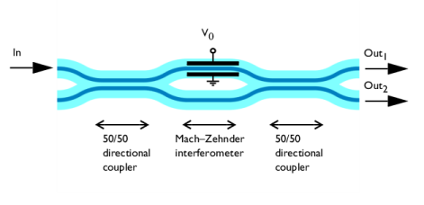
The device in Figure 1 is a Mach–Zehnder modulator. The input wave is launched into a directional coupler. The power of the input is split equally into the two output waveguides of the first directional coupler. Those two waveguides form the two arms of a Mach–Zehnder interferometer. On one of the arms, you can apply an electric field to modify the refractive index in the material and, thus, modify the phase for the wave propagating through that arm. The two waves are then combined into another 50/50 directional coupler. By changing the applied voltage you can continuously control the amount of light exiting from the two output waveguides.
Figure 1: Schematic drawing of the Mach–Zehnder modulator.
A common material for fabricating waveguide modulators is lithium niobate, LiNbO3. Lithium niobate is a ferroelectric crystal that exhibits uniaxial birefringence. Waveguide structures can be fabricated by either indiffusion of Ti into the core regions or by annealed proton exchange, where lithium ions are exchanged with protons from an acid bath.
Model Definition
This application shows how the Electromagnetic Waves, Beam Envelopes interface can be combined with the Electrostatics interface to perform simulations of the properties of an optical waveguide modulator. The model is implemented in a 2D geometry, but could be extended to a full 3D simulation.
The Electromagnetic Waves, Beam Envelopes interface is formulated assuming that the electric field is defined as the product of a slowly varying envelope function and a rapidly varying phase function
where E1 is the envelope function, k is a wave vector and r is the position. If k is properly selected for the problem, the envelope function E1 has a spatial variation occurring on a length scale much larger than the wavelength. A good assumption, for this application, is that the wave is well approximated in the straight domains using the wave vector for the incident mode, β. However, in the waveguide bends the wave vector can be written as
where β = k0neff is the propagation constant for the mode, k0 is the vacuum wave number, neff is the effective index of the waveguide mode, α is the angle from the x-axis, and x and y are the unit vectors in the x and y directions, respectively.
The wave vector difference is thus
It is the wave vector difference that determines the phase variation for the envelope field. Thus, you must make sure that the phase variation is well resolved by the mesh. For instance,
where N is a suitably large number, for instance 6. From the relations above, you get that the maximum mesh element sizes in the x and y directions should be
and
Results and Discussion
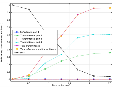
The first part of the application is to define a minimum bend radius that provides low loss. Figure 2 shows the power transmission for an S-shaped bend. As seen, a bend radius of 2.5 mm gives a transmission of approximately 95% of the power. Accept the 5% loss and fix the bend radius to be 2.5 mm.
Figure 2: The transmission through an S-bent waveguide versus the radius of curvature for the bend.
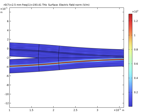
Figure 3 shows the electric field norm for the wave propagating in the S-shaped bend, for a bend radius of 2.5 mm. As seen, the wave follows the waveguide in the bend, as expected.
Figure 3: The electric field norm for the wave in the S-bent waveguide for a radius of curvature of 2.5 mm.
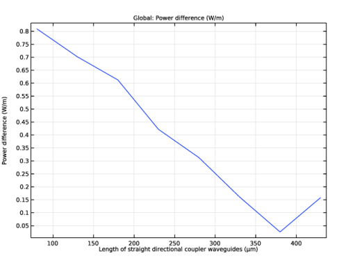
You want the directional coupler structures to operate as 50/50 couplers. That is, half of the incident power should exit from each of the two output arms. To find the coupler length where this condition is met, monitor the power difference in the two arms of the Mach–Zehnder interferometer and sweep the length of the directional coupler. Figure 4 shows the result of the parameter sweep. A coupler length of 380 μm gives zero power difference between the two arms. That is, the power is the same in the two arms.
Figure 4: The absolute value of the power difference between the two waveguide arms in the Mach–Zehnder interferometer versus the length of the directional coupler.
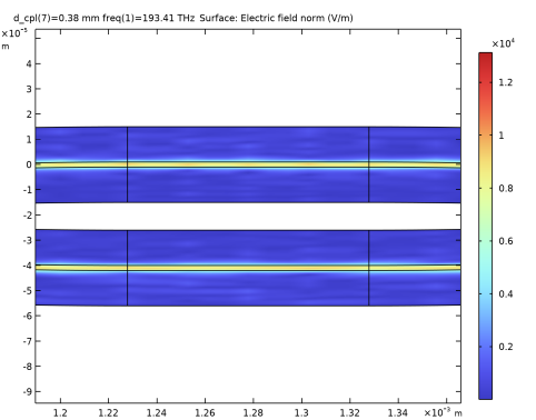
Figure 5 shows that the electric field norms for the two arms indeed seem to be the same.
Figure 5: The electric field norm in the two waveguide arms of the Mach–Zehnder interferometer. As shown, the fields are almost the same for a directional coupler length of 380 μm.
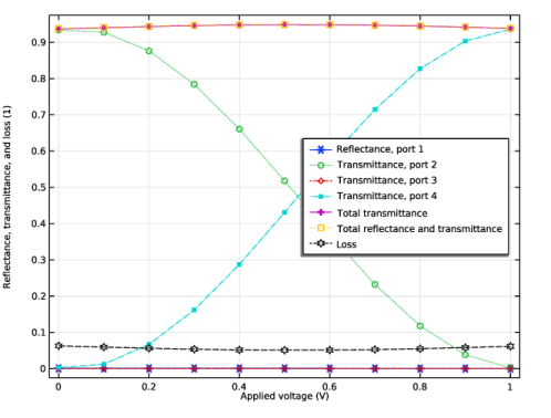
Finally, a voltage is applied across the waveguide in one of the arms. The voltage modifies the refractive index in the arm and, thus, there is a phase difference between the wave propagating through the two Mach–Zehnder interferometer arms. As expected, Figure 6 shows that the wave can be switched between the two output waveguides by tuning the applied voltage. Thus, if all input and output ports are connected to other waveguides or fibers, you can use the device as a spatial switch. However, if only one input port and one output port are active, the device operates as an amplitude modulator.
Figure 6: The transmission to the upper (port 2) and the lower (port 4) output waveguide versus the applied voltage, V0.
Notes About the COMSOL Implementation
The geometry is built using the Wave Optics Module part library, by loading special parts for straight waveguides and directional couplers.
Application Library path: Wave_Optics_Module/Waveguides_and_Couplers/mach_zehnder_modulator
Modeling Instructions
First add the physics interface and the study sequence.
From the File menu, choose New.
New
In the New window, click  Model Wizard.
Model Wizard
1
In the Model Wizard window, click  2D.
2
In the Select Physics tree, select Optics>Wave Optics>Electromagnetic Waves, Beam Envelopes (ewbe).
3
Click Add.
4
Click  Study.
5
In the Select Study tree, select Preset Studies for Selected Physics Interfaces>Boundary Mode Analysis.
6
Global Definitions
First load some parameters from file. The parameters are used when defining the physics and the mesh.
General Parameters
1
In the Model Builder window, under Global Definitions click Parameters 1.
2
In the Settings window for Parameters, type General Parameters in the Label text field.
3
Locate the Parameters section. Click  Load from File.
4
Geometry Parameters
Also load the geometry parameters from file. The parameters define the sizes and locations for the geometric objects.
1
In the Home toolbar, click  Parameters and choose Add>Parameters.
2
In the Settings window for Parameters, type Geometry Parameters in the Label text field.
3
Locate the Parameters section. Click  Load from File.
4
The length of the Mach-Zehnder arms has purposely been set to a small value, to make it easier to build the geometry. You will later change the length to a realistic value.
In a later study, you will optimize the radius of curvature for the S-bends in the directional couplers, to find a value that is a good compromise between insertion loss and device size.
The geometry is built using parts from the Wave Optics Module part library.
First, add a directional coupler part.
Part Libraries
1
In the Home toolbar, click  Windows and choose Part Libraries.
2
In the Part Libraries window, select Wave Optics Module>Slab Waveguides>slab_waveguide_s_bend_directional_coupler in the tree.
3
Click  Add to Geometry.
Geometry 1
Slab Waveguide S-Bend Directional Coupler 1 (pi1)
1
In the Model Builder window, under Component 1 (comp1)>Geometry 1 click Slab Waveguide S-Bend Directional Coupler 1 (pi1).
2
In the Settings window for Part Instance, locate the Input Parameters section.
3
4
Locate the Position and Orientation of Output section. In the Rotation angle text field, type -90.
5
Click  Build All Objects.
6
Click the  Zoom Extents button in the Graphics toolbar.
The part contains pre-defined selections that can be used for assigning selections to boundary conditions, materials and mesh features. Add cumulative selections for the core and the cladding domain selections.
7
Click to expand the Domain Selections section. Click New Cumulative Selection.
8
In the New Cumulative Selection dialog box, type Core in the Name text field.
9
10
In the Settings window for Part Instance, locate the Domain Selections section.
11
Click New Cumulative Selection.
12
In the New Cumulative Selection dialog box, type Cladding in the Name text field.
13
14
In the Settings window for Part Instance, locate the Domain Selections section.
15
Add a new cumulative selection for all exterior boundaries, except the port boundaries.
16
Click to expand the Boundary Selections section. Click New Cumulative Selection.
17
In the New Cumulative Selection dialog box, type Transverse Perimeter in the Name text field.
18
19
In the Settings window for Part Instance, locate the Boundary Selections section.
20
Part Libraries
Next, add a straight waveguide part.
1
In the Home toolbar, click  Windows and choose Part Libraries.
2
In the Part Libraries window, select Wave Optics Module>Slab Waveguides>slab_waveguide_straight in the tree.
3
Click  Add to Geometry.
Geometry 1
Slab Waveguide Straight 1 (pi2)
1
In the Model Builder window, under Component 1 (comp1)>Geometry 1 click Slab Waveguide Straight 1 (pi2).
2
In the Settings window for Part Instance, locate the Input Parameters section.
3
4
Locate the Position and Orientation of Output section. In the x-displacement text field, type -d0.
5
In the Rotation angle text field, type -90.
6
Click  Build All Objects.
7
Click the  Zoom Extents button in the Graphics toolbar.
Again, assign selections from the part to the cumulative core, cladding, and transverse perimeter selections.
8
Locate the Domain Selections section. In the table, enter the following settings:
9
Locate the Boundary Selections section. In the table, enter the following settings:
Slab Waveguide Straight 2 (pi3)
1
Right-click Component 1 (comp1)>Geometry 1>Slab Waveguide Straight 1 (pi2) and choose Duplicate.
2
In the Settings window for Part Instance, locate the Position and Orientation of Output section.
3
In the y-displacement text field, type -d_pcc.
4
Click  Build All Objects.
5
Click the  Zoom Extents button in the Graphics toolbar.
Slab Waveguide Straight 3 (pi4)
1
Right-click Slab Waveguide Straight 1 (pi2) and choose Duplicate.
2
In the Settings window for Part Instance, locate the Input Parameters section.
3
4
Locate the Position and Orientation of Output section. In the x-displacement text field, type d_dc.
5
Click  Build All Objects.
6
Click the  Zoom Extents button in the Graphics toolbar.
Slab Waveguide Straight 4 (pi5)
1
Right-click Slab Waveguide Straight 3 (pi4) and choose Duplicate.
2
In the Settings window for Part Instance, locate the Position and Orientation of Output section.
3
In the y-displacement text field, type -d_pcc.
4
Click  Build All Objects.
5
Click the  Zoom Extents button in the Graphics toolbar.
Slab Waveguide S-Bend Directional Coupler 2 (pi6)
1
In the Model Builder window, under Component 1 (comp1)>Geometry 1 right-click Slab Waveguide S-Bend Directional Coupler 1 (pi1) and choose Duplicate.
2
In the Settings window for Part Instance, locate the Position and Orientation of Output section.
3
In the x-displacement text field, type d_dc+d_mz.
4
Click  Build All Objects.
5
Click the  Zoom Extents button in the Graphics toolbar.
Slab Waveguide Straight 5 (pi7)
1
In the Model Builder window, under Component 1 (comp1)>Geometry 1 right-click Slab Waveguide Straight 1 (pi2) and choose Duplicate.
2
In the Settings window for Part Instance, locate the Position and Orientation of Output section.
3
In the x-displacement text field, type 2*d_dc+d_mz.
4
Click  Build All Objects.
5
Click the  Zoom Extents button in the Graphics toolbar.
Slab Waveguide Straight 6 (pi8)
1
Right-click Slab Waveguide Straight 5 (pi7) and choose Duplicate.
2
In the Settings window for Part Instance, locate the Position and Orientation of Output section.
3
In the y-displacement text field, type -d_pcc.
4
Click  Build All Objects.
5
Click the  Zoom Extents button in the Graphics toolbar.
Slab Waveguide Straight 2 (pi3)
Now, add selections for the port boundaries.
1
In the Model Builder window, click Slab Waveguide Straight 2 (pi3).
2
In the Settings window for Part Instance, locate the Boundary Selections section.
3
Click New Cumulative Selection.
4
In the New Cumulative Selection dialog box, type Port 1 in the Name text field.
5
6
In the Settings window for Part Instance, locate the Boundary Selections section.
7
Slab Waveguide Straight 5 (pi7)
1
In the Model Builder window, click Slab Waveguide Straight 5 (pi7).
2
In the Settings window for Part Instance, locate the Boundary Selections section.
3
Click New Cumulative Selection.
4
In the New Cumulative Selection dialog box, type Port 2 in the Name text field.
5
6
In the Settings window for Part Instance, locate the Boundary Selections section.
7
Slab Waveguide Straight 1 (pi2)
1
In the Model Builder window, click Slab Waveguide Straight 1 (pi2).
2
In the Settings window for Part Instance, locate the Boundary Selections section.
3
Click New Cumulative Selection.
4
In the New Cumulative Selection dialog box, type Port 3 in the Name text field.
5
6
In the Settings window for Part Instance, locate the Boundary Selections section.
7
Slab Waveguide Straight 6 (pi8)
1
In the Model Builder window, click Slab Waveguide Straight 6 (pi8).
2
In the Settings window for Part Instance, locate the Boundary Selections section.
3
Click New Cumulative Selection.
4
In the New Cumulative Selection dialog box, type Port 4 in the Name text field.
5
6
In the Settings window for Part Instance, locate the Boundary Selections section.
7
Slab Waveguide Straight 3 (pi4)
Add two selections that later will be used by integration operators.
1
In the Model Builder window, click Slab Waveguide Straight 3 (pi4).
2
In the Settings window for Part Instance, locate the Boundary Selections section.
3
Click New Cumulative Selection.
4
In the New Cumulative Selection dialog box, type End of Upper Mach-Zehnder Waveguide in the Name text field.
5
6
In the Settings window for Part Instance, locate the Boundary Selections section.
7
Slab Waveguide Straight 4 (pi5)
1
In the Model Builder window, click Slab Waveguide Straight 4 (pi5).
2
In the Settings window for Part Instance, locate the Boundary Selections section.
3
Click New Cumulative Selection.
4
In the New Cumulative Selection dialog box, type End of Lower Mach-Zehnder Waveguide in the Name text field.
5
6
In the Settings window for Part Instance, locate the Boundary Selections section.
7
Edge Mesh
1
In the Geometry toolbar, click  Selections and choose Union Selection.
2
In the Settings window for Union Selection, type Edge Mesh in the Label text field. This selection will be used later when defining the selection for an edge mesh feature.
3
Locate the Geometric Entity Level section. From the Level list, choose Boundary.
4
Locate the Input Entities section. Click  Add.
5
In the Add dialog box, in the Selections to add list, choose Port 1 and Port 3.
6
Materials
Define the materials for the waveguide structure.
Cladding
1
In the Model Builder window, under Component 1 (comp1) right-click Materials and choose Blank Material.
2
In the Settings window for Material, type Cladding in the Label text field.
3
Locate the Material Contents section. In the table, enter the following settings:
Core
1
Right-click Materials and choose Blank Material.
2
In the Settings window for Material, type Core in the Label text field.
3
Locate the Geometric Entity Selection section. From the Selection list, choose Core.
4
Locate the Material Contents section. In the table, enter the following settings:
Electromagnetic Waves, Beam Envelopes (ewbe)
Set up the interface for unidirectional propagation, using the wave number calculated in the boundary mode analysis.
1
In the Model Builder window, under Component 1 (comp1) click Electromagnetic Waves, Beam Envelopes (ewbe).
2
In the Settings window for Electromagnetic Waves, Beam Envelopes, locate the Components section.
3
From the Electric field components solved for list, choose Out-of-plane vector.
4
Locate the Wave Vectors section. From the Number of directions list, choose Unidirectional.
5
Specify the k1 vector as
Port 1
Now define the input and the output ports, using the previously defined selections.
1
In the Physics toolbar, click  Boundaries and choose Port.
2
In the Settings window for Port, locate the Boundary Selection section.
3
From the Selection list, choose Port 1.
4
Locate the Port Properties section. From the Type of port list, choose Numeric.
For the first port, wave excitation is On by default.
Port 2
1
In the Physics toolbar, click  Boundaries and choose Port.
2
In the Settings window for Port, locate the Boundary Selection section.
3
From the Selection list, choose Port 2.
4
Locate the Port Properties section. From the Type of port list, choose Numeric.
Port 3
1
In the Physics toolbar, click  Boundaries and choose Port.
2
In the Settings window for Port, locate the Boundary Selection section.
3
From the Selection list, choose Port 3.
4
Locate the Port Properties section. From the Type of port list, choose Numeric.
Port 4
1
In the Physics toolbar, click  Boundaries and choose Port.
2
In the Settings window for Port, locate the Boundary Selection section.
3
From the Selection list, choose Port 4.
4
Locate the Port Properties section. From the Type of port list, choose Numeric.
Scattering Boundary Condition 1
Use the scattering boundary condition to absorb some of the light that is not guided by the waveguide. The scattering boundary condition is only absorbing light propagating close to the normal direction to the boundary, so it will not absorb unguided light propagating with large angles of incidence.
1
In the Physics toolbar, click  Boundaries and choose Scattering Boundary Condition.
2
In the Settings window for Scattering Boundary Condition, locate the Boundary Selection section.
3
From the Selection list, choose Transverse Perimeter.
Mesh 1
Define a mesh on the edge and then map it over the whole domain.
1
In the Model Builder window, under Component 1 (comp1) click Mesh 1.
2
In the Settings window for Mesh, locate the Physics-Controlled Mesh section.
3
In the table, clear the Use check box for Electromagnetic Waves, Beam Envelopes (ewbe).
4
Locate the Sequence Type section. From the list, choose User-controlled mesh.
Free Triangular 1
In the Model Builder window, under Component 1 (comp1)>Mesh 1 right-click Free Triangular 1 and choose Delete. Click Yes to confirm.
Edge 1
1
In the Mesh toolbar, click  Edge.
2
In the Settings window for Edge, locate the Boundary Selection section.
3
From the Selection list, choose Edge Mesh.
Size 1
1
Right-click Edge 1 and choose Size.
2
In the Settings window for Size, locate the Element Size section.
3
Click the Custom button.
4
Locate the Element Size Parameters section.
5
Select the Maximum element size check box. In the associated text field, type hy.
Size 2
1
In the Model Builder window, right-click Edge 1 and choose Size.
2
In the Settings window for Size, locate the Geometric Entity Selection section.
3
Click  Clear Selection.
4
5
Locate the Element Size section. Click the Custom button.
6
Locate the Element Size Parameters section.
7
Select the Maximum element size check box. In the associated text field, type min(hy,w/4).
Mapped 1
1
In the Mesh toolbar, click  Mapped.
2
In the Settings window for Mapped, click to expand the Reduce Element Skewness section.
3
Select the Adjust edge mesh check box.
Size 1
1
Right-click Mapped 1 and choose Size.
2
In the Settings window for Size, locate the Element Size section.
3
Click the Custom button.
4
Locate the Element Size Parameters section.
5
Select the Maximum element size check box. In the associated text field, type hx.
6
Click  Build All.
Study 1
Step 1: Boundary Mode Analysis
Now define the boundary mode analysis study steps for the numeric ports and the frequency domain study for finding the domain solution.
1
In the Model Builder window, under Study 1 click Step 1: Boundary Mode Analysis.
2
In the Settings window for Boundary Mode Analysis, locate the Study Settings section.
3
In the Mode analysis frequency text field, type f0.
4
Select the Search for modes around check box. In the associated text field, type n_core.
Step 3: Boundary Mode Analysis 1
1
Right-click Study 1>Step 1: Boundary Mode Analysis and choose Duplicate.
2
In the Settings window for Boundary Mode Analysis, locate the Study Settings section.
3
In the Port name text field, type 2.
Step 4: Boundary Mode Analysis 2
1
Right-click Step 3: Boundary Mode Analysis 1 and choose Duplicate.
2
In the Settings window for Boundary Mode Analysis, locate the Study Settings section.
3
In the Port name text field, type 3.
Step 5: Boundary Mode Analysis 3
1
Right-click Step 4: Boundary Mode Analysis 2 and choose Duplicate.
2
In the Settings window for Boundary Mode Analysis, locate the Study Settings section.
3
In the Port name text field, type 4.
Step 2: Frequency Domain
1
In the Model Builder window, click Step 2: Frequency Domain.
2
In the Settings window for Frequency Domain, locate the Study Settings section.
3
In the Frequencies text field, type f0.
4
Right-click Study 1>Step 2: Frequency Domain and choose Move Down three times, or simply drag and drop the frequency domain study step to the last position.
5
In the Home toolbar, click  Compute.
Results
Plots of the mode fields are automatically generated, when numeric ports are used. Inspect the mode field for the first port.
Electric Mode Field, Port 1 (ewbe)
Electric Field (ewbe)
1
In the Model Builder window, click Electric Field (ewbe).
2
As seen from the result graph, the wave is not bound to the core when the bend radius is so small. To make the wave follow the waveguide core, the bend radius must be increased. Thus, make a parametric sweep of the bend radius to find the smallest radius that gives a sufficient transmission.
Study 1
Parametric Sweep
1
In the Study toolbar, click  Parametric Sweep.
2
In the Settings window for Parametric Sweep, locate the Study Settings section.
3
4
From the list in the Parameter name column, choose r0 (Bend radius).
5
Click  Range.
6
In the Range dialog box, type 0.1[mm] in the Start text field.
7
In the Step text field, type 0.4[mm].
8
In the Stop text field, type 2.5[mm].
9
Click Replace.
10
In the Settings window for Parametric Sweep, locate the Study Settings section.
11
12
In the Study toolbar, click  Compute.
Results
Reflectance, Transmittance, and Loss (ewbe)
Replace absorptance with loss in the plot label, the y-axis label and the plot legend, as this is more appropriate here as the loss is due to waveguide loss - not material absorption.
1
In the Model Builder window, under Results click Reflectance, Transmittance, and Absorptance (ewbe).
2
In the Settings window for 1D Plot Group, type Reflectance, Transmittance, and Loss (ewbe) in the Label text field.
3
Locate the Plot Settings section. In the y-axis label text field, type Reflectance, transmittance, and loss (1).
Global 1
1
In the Model Builder window, expand the Reflectance, Transmittance, and Loss (ewbe) node, then click Global 1.
2
In the Settings window for Global, locate the y-Axis Data section.
3
Add markers and use different line types, to make it easier to distinguish the different curves.
4
Click to expand the Coloring and Style section. Find the Line style subsection. From the Line list, choose Cycle.
5
Find the Line markers subsection. From the Marker list, choose Cycle.
Reflectance, Transmittance, and Loss (ewbe)
1
In the Model Builder window, click Reflectance, Transmittance, and Loss (ewbe).
2
In the Settings window for 1D Plot Group, locate the Legend section.
3
From the Position list, choose Middle left. Your graph should look the same as the graph in Figure 2. A loss of approximately 5% seems reasonable, which you get for a bend radius of 2.5 mm.
Electric Field (ewbe) 1
1
In the Model Builder window, click Electric Field (ewbe) 1.
2
3
In the Electric Field (ewbe) 1 toolbar, click  Plot. Compare your graph to Figure 3. As you see, for a 2.5 mm bend radius, the wave is bound to the waveguide core. Thus, now set the bend radius parameter to 2.5 mm.
Global Definitions
Geometry Parameters
1
In the Model Builder window, under Global Definitions click Geometry Parameters.
2
In the Settings window for Parameters, locate the Parameters section.
3
Definitions
Now make sure that the directional coupler splits power of the incoming wave equally much into its output ports. To do this, compare the power in the two waveguide arms of the Mach–Zehnder interferometer.
Integration 1 (intop1)
1
In the Definitions toolbar, click  Nonlocal Couplings and choose Integration.
2
In the Settings window for Integration, locate the Source Selection section.
3
From the Geometric entity level list, choose Boundary.
4
From the Selection list, choose End of Upper Mach-Zehnder Waveguide.
5
Click  Zoom to Selection.
Integration 2 (intop2)
1
Right-click Integration 1 (intop1) and choose Duplicate.
2
In the Settings window for Integration, locate the Source Selection section.
3
From the Selection list, choose End of Lower Mach-Zehnder Waveguide.
4
Click  Zoom to Selection.
Variables 1
1
In the Definitions toolbar, click  Local Variables.
2
In the Settings window for Variables, locate the Variables section.
3
Study 1
Parametric Sweep
Modify the parametric sweep for a sweep of the directional coupler length.
1
In the Model Builder window, under Study 1 click Parametric Sweep.
2
In the Settings window for Parametric Sweep, locate the Study Settings section.
3
From the list in the Parameter name column, choose d_cpl (Length of straight directional coupler waveguides).
4
Click  Range.
5
In the Range dialog box, type 80[um] in the Start text field.
6
In the Step text field, type 50[um].
7
In the Stop text field, type 430[um].
8
Click Replace.
9
In the Home toolbar, click  Compute.
Results
First, inspect the results for the transmittances and the loss.
Global 1
1
In the Model Builder window, under Results>Reflectance, Transmittance, and Loss (ewbe) click Global 1.
2
In the Settings window for Global, locate the x-Axis Data section.
3
In the Expression text field, type d_cpl.
4
From the Unit list, choose µm.
Reflectance, Transmittance, and Loss (ewbe)
1
In the Model Builder window, click Reflectance, Transmittance, and Loss (ewbe).
2
In the Settings window for 1D Plot Group, locate the Legend section.
3
From the Position list, choose Middle right.
4
In the Reflectance, Transmittance, and Loss (ewbe) toolbar, click  Plot.
As this plot does not answer the question whether the powers in the upper and lower waveguides are equal, create a new 1D plot.
Power Difference
1
In the Home toolbar, click  Add Plot Group and choose 1D Plot Group.
2
In the Settings window for 1D Plot Group, type Power Difference in the Label text field.
3
Locate the Data section. From the Dataset list, choose Study 1/Parametric Solutions 1 (sol6).
Global 1
1
Right-click Power Difference and choose Global.
2
In the Settings window for Global, locate the y-Axis Data section.
3
4
Locate the x-Axis Data section. From the Axis source data list, choose Outer solutions.
5
From the Parameter list, choose Expression.
6
In the Expression text field, type d_cpl.
7
From the Unit list, choose µm.
Power Difference
1
In the Model Builder window, click Power Difference.
2
In the Settings window for 1D Plot Group, locate the Legend section.
3
Clear the Show legends check box.
4
In the Power Difference toolbar, click  Plot. Your graph should now look like Figure 4.
Electric Field (ewbe) 1
1
In the Model Builder window, click Electric Field (ewbe) 1.
2
In the Electric Field (ewbe) 1 toolbar, click  Plot.
3
Click the  Zoom Extents button in the Graphics toolbar.
4
Click the  Zoom In button in the Graphics toolbar four times. Your plot should now look like Figure 5.
Global Definitions
As shown in Figure 4 and Figure 5, the power in the two waveguides is almost the same when the directional coupler waveguides are 380 μm long. Thus, set the parameter d_cpl to 380 μm.
Geometry Parameters
1
In the Model Builder window, under Global Definitions click Geometry Parameters.
2
In the Settings window for Parameters, locate the Parameters section.
3
The final geometry parameter to fix is the Mach–Zehnder waveguide length. Set it to 2 cm.
4
Component 1 (comp1)
Finally, add an Electrostatics user interface to apply an electric field across the waveguide in one of the arms of the interferometer.
Add Physics
1
In the Home toolbar, click  Add Physics to open the Add Physics window.
2
Go to the Add Physics window.
3
In the tree, select AC/DC>Electric Fields and Currents>Electrostatics (es).
4
Click Add to Component 1 in the window toolbar.
5
In the Home toolbar, click  Add Physics to close the Add Physics window.
Materials
Cladding (mat1)
1
In the Model Builder window, under Component 1 (comp1)>Materials click Cladding (mat1).
2
In the Settings window for Material, locate the Material Contents section.
3
Right-click the Relative permittivity row and choose Edit.
4
In the Relative permittivity dialog box, choose Isotropic from the list.
5
6
Core (mat2)
1
In the Model Builder window, click Core (mat2).
2
In the Settings window for Material, locate the Material Contents section.
3
Right-click the Relative permittivity row and choose Edit.
4
In the Relative permittivity dialog box, choose Isotropic from the list.
5
6
Geometry 1
Add two lines for the terminals - one for the ground and one for the applied voltage.
Polygon 1 (pol1)
1
In the Geometry toolbar, click  Polygon.
2
In the Settings window for Polygon, locate the Coordinates section.
3
Polygon 2 (pol2)
1
Right-click Polygon 1 (pol1) and choose Duplicate.
2
In the Settings window for Polygon, locate the Coordinates section.
3
4
Click  Build All Objects.
5
Electrostatics (es)
Now, add a voltage terminal and a ground.
In the Model Builder window, under Component 1 (comp1) click Electrostatics (es).
Electric Potential 1
1
In the Physics toolbar, click  Boundaries and choose Electric Potential.
2
3
In the Settings window for Electric Potential, locate the Electric Potential section.
4
In the V0 text field, type V0.
Ground 1
1
In the Physics toolbar, click  Boundaries and choose Ground.
2
Materials
Cladding (mat1)
Also make sure that the refractive index is changed by the applied static electric field.
1
In the Model Builder window, under Component 1 (comp1)>Materials click Cladding (mat1).
2
In the Settings window for Material, locate the Material Contents section.
3
Core (mat2)
1
In the Model Builder window, click Core (mat2).
2
In the Settings window for Material, locate the Material Contents section.
3
Study 1
Parametric Sweep
1
In the Model Builder window, under Study 1 click Parametric Sweep.
2
In the Settings window for Parametric Sweep, locate the Study Settings section.
3
From the list in the Parameter name column, choose V0 (Applied voltage).
4
Click  Range.
5
In the Range dialog box, type 0[V] in the Start text field.
6
In the Step text field, type 0.1[V].
7
In the Stop text field, type 1[V].
8
Click Replace.
Stationary
1
In the Study toolbar, click  Study Steps and choose Stationary>Stationary.
2
Right-click Study 1>Step 6: Stationary and choose Move Up.
Step 6: Frequency Domain
1
In the Model Builder window, click Step 6: Frequency Domain.
2
In the Settings window for Frequency Domain, locate the Physics and Variables Selection section.
3
In the table, clear the Solve for check box for Electrostatics (es).
4
In the Study toolbar, click  Compute.
Results
Global 1
1
In the Model Builder window, under Results>Reflectance, Transmittance, and Loss (ewbe) click Global 1.
2
In the Settings window for Global, locate the x-Axis Data section.
3
In the Expression text field, type V0.
4
In the Reflectance, Transmittance, and Loss (ewbe) toolbar, click  Plot. Compare your graph with Figure 6.