PDF

DC Characteristics of a MOS Transistor (MOSFET)
This model calculates the DC characteristics of a MOS (metal-oxide semiconductor) transistor. In normal operation, a system turns on a MOS transistor by applying a voltage to the gate electrode. When the voltage on the drain increases, the drain current also increases until it reaches saturation. The saturation current depends on the gate voltage.
Introduction
The MOSFET (metal oxide semiconductor field-effect transistor) is by far the most common semiconductor device, and it is the primary building block in all commercial processors, memories, and digital integrated circuits. Since the first microprocessors were introduced approximately 40 years ago this device has experienced tremendous development, and today it is being manufactured with feature sizes of 22 nm and smaller.
The MOSFET is essentially a miniaturized switch. In this example the source and drain contacts (the input and output of the switch) are both ohmic (low resistance) contacts to heavily doped n-type regions of the device. Between these two contacts is a region of p-type semiconductor. The gate contact lies above the p-type semiconductor, slightly overlapping the two n-type regions. It is separated from the semiconductor by a thin layer of Silicon oxide, so that it forms a capacitor with the underlying semiconductor. Applying a voltage to the gate changes the local band structure beneath it through the Field Effect. A sufficiently high voltage can cause the semiconductor to change from p-type to n-type in a thin layer (the channel) underneath the gate. This is known as inversion and the channel is sometimes referred to as the inversion layer. The channel connects the two n-type regions of semiconductor with a thin n-type region under the gate. This region has a significantly lower resistance than the series resistance of the np/pn junctions that separated the source and the gate before the gate voltage produced the inversion layer. Consequently applying a gate voltage can be used to change the resistance of the device from a high to a low value. The gate voltage where a significant current begins to flow is called the threshold or turn-on voltage. Figure 1 shows a schematic MOSFET with the main electrical connections highlighted. Figure 2 shows an electron microscope image of a modern MOSFET device.
Figure 1: Schematic diagram of a typical MOSFET. The current flows from the source to the gate through a channel underneath the gate. The size of the channel is controlled by the gate voltage.
Figure 2: Cross-section TEM (transmission electron microscopy) image of a 50 nm gate length MOSFET fabricated at KTH Electrum laboratory by P.E Hellström and coworkers within the ERC advanced grant OSIRIS research project headed by Prof. M. Östling.
As the voltage between the drain and the source is increased the current carried by the channel eventually saturates through a process known as pinch-off, in which the channel narrows at one end due to the effect of the field parallel to the surface. The channel width is controlled by the gate voltage. Typically a larger gate voltage results in wider channel and consequently a lower resistance for a given drain voltage. Additionally the saturation current is larger for a higher gate voltage.
Model Definition
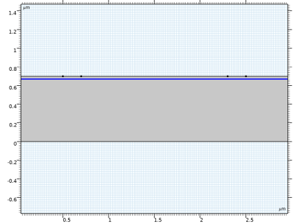
Figure 3 shows the model geometry, indicating how the geometry elements correspond to features in Figure 1 In this model both the source and the base are connected to ground and the voltages applied to the drain and the gate are varied. In the first study a small voltage (10 mV) is applied to the Drain and the Gate voltage is swept from 0 to 5 V. A plot of the current flowing between the source and the drain is used to determine the turn-on voltage of the device. The second study sweeps the drain voltage from 0 to V at three different values of the gate voltage (2, 3, and 4 V). The drain current vs. drain voltage is then plotted at several values of the gate voltage.
Figure 3: Model geometry showing the external connections.
Results and Discussion
Figure 4 shows the drain current vs gate voltage for a fixed drain voltage of 10 mV. From the plot it is clear that the threshold voltage, VT, of the transistor is approximately 1.2 V. It is possible to compare this value with the theoretical value given in Ref. 1:
where dox is the thickness of the oxide and εr,ox is its relative permittivity, ε0 is the permittivity of free space, εr,s is the relative permittivity of the semiconductor, q is the electron charge, and Na is the acceptor concentration under the gate. The flat band voltage VFB and the potential difference between the intrinsic level and the Fermi-level, ΨB, are given by the following equations:
where Φm is the work function of the metal contact, χ is the semiconductor electron affinity, kB is Boltzmann’s contact, T is the absolute temperature, Nc is the semiconductor density of states in the conduction band, and ni is the intrinsic carrier density. The equilibrium electron (neq) and hole (peq) densities are given by:
where Nd is the donor concentration under the gate. Note that these equations assume both complete ionization and Maxwell Boltzmann statistics (reasonable assumptions in the region under the gate). These equations give a threshold voltage of 1.18 V, in good agreement with the simulation value given the approximations required for the analytic approach.
Figure 4: Drain current vs. gate voltage shown when a voltage of 10 mV is applied to the drain. The threshold voltage is approximately 1.2 V.
Figure 5 shows the drain current vs drain voltage curves for different values of the gate voltage. The curve shows three regions: a linear region at low voltages, a nonlinear region at intermediate voltages and an approximately constant region at higher voltages (the saturation region). For this device there is a slight gradient in the current at larger voltages due to the onset of short channel effects. Short channel effects mean that the standard analytic expressions for the saturation voltage and current are inaccurate, but the saturation voltages are of a similar magnitude to those predicted by the simple theory given in Ref. 1. The current saturation occurs due to a phenomenon known as pinch–off. As the drain voltage is increased more current flows along the channel and the potential drop along its length increases. The voltage between the gate and the semiconductor therefore changes as a function of position along the channel and the inversion layer width is no longer constant. Figure 6 shows the electron concentration and the electric potential at different values of the drain voltage for a gate voltage of 4 V. The pinch–off effect is apparent at 5 V.
Figure 5: Drain current vs drain voltage for different values of the gate voltage.
Figure 6: Left: Electron concentration and Right: Electric Potential for the MOSFET with an applied gate voltage of 4 V and with various applied drain voltages, Vd. Top: Vd=5 V, Middle: Vd=1 V, Bottom: Vd=0 V. The pinch-off effect is apparent from the plots.
Reference
1. S. M. Sze and K.K. Ng, Physics of Semiconductor Devices, 3rd ed., John Wiley & Sons, pp. 305–306, 2007.
Application Library path: Semiconductor_Module/Transistors/mosfet
Modeling Instructions
From the File menu, choose New.
New
In the New window, click  Model Wizard.
Model Wizard
1
In the Model Wizard window, click  2D.
2
In the Select Physics tree, select Semiconductor>Semiconductor (semi).
3
Click Add.
4
Click  Study.
5
In the Select Study tree, select General Studies>Stationary.
6
Global Definitions
Define parameters for the drain and gate voltages that you will later use when performing parametric sweeps.
Parameters 1
1
In the Model Builder window, under Global Definitions click Parameters 1.
2
In the Settings window for Parameters, locate the Parameters section.
3
Geometry 1
The geometry can be specified using COMSOL’s built in tools. First choose to define geometry objects using micrometer units.
1
In the Model Builder window, under Component 1 (comp1) click Geometry 1.
2
In the Settings window for Geometry, locate the Units section.
3
From the Length unit list, choose µm.
Next create a rectangle to define the geometry extents.
Rectangle 1 (r1)
1
In the Geometry toolbar, click  Rectangle.
2
In the Settings window for Rectangle, locate the Size and Shape section.
3
In the Width text field, type 3.
4
In the Height text field, type 0.7.
Add a polygon which will include points to define the source, drain and gate contacts. It will also include a line to help create the mesh.
Polygon 1 (pol1)
1
In the Geometry toolbar, click  Polygon.
2
In the Settings window for Polygon, locate the Object Type section.
3
From the Type list, choose Closed curve.
4
Locate the Coordinates section. In the table, enter the following settings:
Mesh Control Edges 1 (mce1)
1
In the Geometry toolbar, click  Virtual Operations and choose Mesh Control Edges.
2
On the object fin, select Boundary 4 only.
It might be easier to select the correct boundary by using the Selection List window. To open this window, in the Home toolbar click Windows and choose Selection List. (If you are running the cross-platform desktop, you find Windows in the main menu.)
3
Right-click Mesh Control Edges 1 (mce1) and choose Build All Objects.
Use the Zoom Extents button to zoom to the full geometry if desired.
4
Click the  Zoom Extents button in the Graphics toolbar.
Materials
Next the material properties are added to the model.
Add Material
1
In the Home toolbar, click  Add Material to open the Add Material window.
2
Go to the Add Material window.
3
In the tree, select Semiconductors>Si - Silicon.
4
Click Add to Component in the window toolbar.
5
In the Home toolbar, click  Add Material to close the Add Material window.
Semiconductor (semi)
Next the physics settings must be defined. Start by defining the doping.
1
In the Model Builder window, under Component 1 (comp1) click Semiconductor (semi).
2
In the Settings window for Semiconductor, locate the Model Properties section.
3
From the Carrier statistics list, choose Fermi-Dirac.
Analytic Doping Model 1
1
In the Physics toolbar, click  Domains and choose Analytic Doping Model.
First a constant background acceptor concentration is defined.
2
In the Settings window for Analytic Doping Model, locate the Impurity section.
3
In the NA0 text field, type 1e17[1/cm^3].
4
Locate the Domain Selection section. From the Selection list, choose All domains.
Add a second doping feature to define the implanted doping profile for the source.
Analytic Doping Model 2
1
In the Physics toolbar, click  Domains and choose Analytic Doping Model.
2
In the Settings window for Analytic Doping Model, locate the Domain Selection section.
3
From the Selection list, choose All domains.
4
Locate the Distribution section. From the list, choose Box.
When defining a Gaussian doping distribution a rectangular region of constant doping is defined. The Gaussian drop off occurs away from the edges of this rectangular region.
First define the location of the lower left corner of the uniformly doped region.
5
Locate the Uniform Region section. Specify the r0 vector as
Then define the width and height of the uniformly doped region.
6
In the W text field, type 0.6[um].
7
In the D text field, type 0.1[um].
Choose the dopant type and the doping level in the uniformly doped region.
8
Locate the Impurity section. From the Impurity type list, choose Donor doping (n-type).
9
In the ND0 text field, type 1e20[1/cm^3].
Next specify the length scale over which the Gaussian drop off occurs. If doping into a background dopant distribution of opposite type (as in this case), this setting specifies the junction depth. In this model different length scales are used in the x and y directions.
10
Locate the Profile section. Select the Specify different length scales for each direction check box.
11
Specify the dj vector as
Finally specify the constant background doping level.
12
From the Nb list, choose Acceptor concentration (semi/adm1).
Add a similar Gaussian doping profile for the drain.
Analytic Doping Model 3
1
Right-click Analytic Doping Model 2 and choose Duplicate.
2
In the Settings window for Analytic Doping Model, locate the Uniform Region section.
3
Specify the r0 vector as
Next set up boundary conditions for the contacts and gate.
First add a contact for the source.
Metal Contact 1
1
In the Physics toolbar, click  Boundaries and choose Metal Contact.
The Metal Contact feature is used to define Metal-Semiconductor interfaces of various types. In this instance, use the default Ideal ohmic contact to define the source.
2
Note that the Metal Contact feature in COMSOL Multiphysics is a so-called Terminal boundary condition. By default a fixed potential of 0 V is applied, which is appropriate in this instance, since the source is grounded. The terminal can also be set up to specify an input current, input power, or to connect to a voltage or current source from an external circuit.
Add a second Metal Contact feature to define the drain.
Metal Contact 2
1
In the Physics toolbar, click  Boundaries and choose Metal Contact.
2
Set the drain voltage to be determined by the previously defined parameter.
3
In the Settings window for Metal Contact, locate the Terminal section.
4
In the V0 text field, type Vd.
Add a third Metal Contact to set the body voltage to 0 V.
Metal Contact 3
1
In the Physics toolbar, click  Boundaries and choose Metal Contact.
2
Set up the gate. The gate dielectric is not explicitly represented in the model, instead the Thin Insulator Gate boundary condition represents both the gate contact and the thin layer of oxide.
Thin Insulator Gate 1
1
In the Physics toolbar, click  Boundaries and choose Thin Insulator Gate.
The Thin Insulator Gate feature is also a terminal, but in this instance it is possible to fix the voltage or charge on the terminal, as well as to connect it to a circuit. Note that the charge setting determines the charge on the conductor and does not relate to trapped charge at the oxide-semiconductor interface.
The voltage applied to the gate is determined by the parameter previously added.
2
In the Settings window for Thin Insulator Gate, locate the Terminal section.
3
In the V0 text field, type Vg.
4
Locate the Gate Contact section. In the εins text field, type 4.5.
5
In the dins text field, type 30[nm].
6
A range of recombination/generation mechanisms are available to be added to the model. In this case, simply add trap-assisted recombination, using the default Shockley-Read-Hall model.
Trap-Assisted Recombination 1
1
In the Physics toolbar, click  Domains and choose Trap-Assisted Recombination.
2
In the Settings window for Trap-Assisted Recombination, locate the Domain Selection section.
3
From the Selection list, choose All domains.
Semiconductor Material Model 1
1
In the Model Builder window, click Semiconductor Material Model 1.
2
In the Settings window for Semiconductor Material Model, click to expand the Band Gap Narrowing section.
3
From the Band gap narrowing list, choose Jain-Roulston model.
We will use a user-defined mesh for this model.
Mesh 1
1
In the Model Builder window, under Component 1 (comp1) click Mesh 1.
2
In the Settings window for Mesh, locate the Sequence Type section.
3
From the list, choose User-controlled mesh.
Size
1
In the Model Builder window, under Component 1 (comp1)>Mesh 1 click Size.
2
In the Settings window for Size, locate the Element Size section.
3
Click the Custom button.
4
Locate the Element Size Parameters section. In the Maximum element growth rate text field, type 1.05.
Size 1
In the Model Builder window, under Component 1 (comp1)>Mesh 1 right-click Size 1 and choose Delete.
Size 2
In the Model Builder window, right-click Size 2 and choose Delete.
Free Triangular 1
In the Model Builder window, right-click Free Triangular 1 and choose Delete.
Edge 1
1
In the Mesh toolbar, click  Edge.
2
3
In the Settings window for Edge, click to expand the Control Entities section.
4
Clear the Smooth across removed control entities check box.
Size 1
1
Right-click Edge 1 and choose Size.
2
In the Settings window for Size, locate the Element Size section.
3
From the Calibrate for list, choose Semiconductor.
4
Click the Custom button.
5
Locate the Element Size Parameters section.
6
Select the Maximum element size check box. In the associated text field, type 0.03.
Mapped 1
1
In the Mesh toolbar, click  Mapped.
2
In the Settings window for Mapped, locate the Domain Selection section.
3
From the Geometric entity level list, choose Domain.
4
5
Click to expand the Control Entities section. Clear the Smooth across removed control entities check box.
6
Click to expand the Reduce Element Skewness section. Select the Adjust edge mesh check box.
Distribution 1
1
Right-click Mapped 1 and choose Distribution.
2
3
In the Settings window for Distribution, locate the Distribution section.
4
From the Distribution type list, choose Predefined.
5
In the Number of elements text field, type 8.
6
In the Element ratio text field, type 9.
7
From the Growth rate list, choose Exponential.
8
Select the Reverse direction check box.
Free Triangular 1
1
In the Mesh toolbar, click  Free Triangular.
2
In the Settings window for Free Triangular, click to expand the Control Entities section.
3
Clear the Smooth across removed control entities check box.
4
Click  Build All.
5
Click the  Zoom Extents button in the Graphics toolbar.
The user-defined mesh is shown in the image below. The mapped mesh with the specific distribution helps create layers of thin elements underneath the gate, where the large gradient of the carrier concentration needs to be resolved by the mesh.
Study 1
Before setting up the study, check that the doping was set up correctly. To do this, first get the initial value for the study.
1
In the Model Builder window, click Study 1.
2
In the Settings window for Study, locate the Study Settings section.
3
Clear the Generate default plots check box.
Disable the default plots since these are not required.
4
In the Study toolbar, click  Get Initial Value.
Results
Add a 2D plot group to check the dopant distribution in the model.
2D Plot Group 1
In the Home toolbar, click  Add Plot Group and choose 2D Plot Group.
Surface 1
1
Right-click 2D Plot Group 1 and choose Surface.
Plot the signed dopant concentration (Nd-Na). This quantity is positive for net donor doping and negative for net acceptor doping.
2
In the Settings window for Surface, locate the Expression section.
3
In the Expression text field, type semi.Nd-semi.Na.
4
In the Unit field, type 1/cm^3.
5
In the 2D Plot Group 1 toolbar, click  Plot.
6
Click the  Zoom Extents button in the Graphics toolbar.
The doping distribution is shown below.
Signed Dopant Concentration
1
In the Model Builder window, right-click 2D Plot Group 1 and choose Rename.
2
In the Rename 2D Plot Group dialog box, type Signed Dopant Concentration in the New label text field.
3
Study 1
Step 1: Stationary
Now set up a Stationary study to determine the turn-on voltage for the transistor. In this study, set Vd to 10 mV and sweep over Vg.
1
In the Model Builder window, under Study 1 click Step 1: Stationary.
2
In the Settings window for Stationary, click to expand the Study Extensions section.
The study extensions panel can be used to set up a parametric sweep.
3
Select the Auxiliary sweep check box.
4
From the Sweep type list, choose All combinations.
Choose all combinations for the sweep to sweep over every combination of the specified parameters.
5
6
The drain voltage is fixed at a constant value.
7
8
The gate voltage is swept between 0 and 4 V with uneven step sizes to reduce computation time and file size.
Running continuation for the Vg parameter configures the solver to use the solution for the previous continuation parameter step as the initial guess for the solution. It also allows the solver to take intermediate steps at values of Vg not specified in the list if necessary.
9
In the Home toolbar, click  Compute.
Results
Add a 1D plot group to plot the source current versus the gate voltage.
1D Plot Group 2
1
In the Home toolbar, click  Add Plot Group and choose 1D Plot Group.
2
In the Settings window for 1D Plot Group, locate the Legend section.
3
From the Position list, choose Upper left.
Global 1
1
Right-click 1D Plot Group 2 and choose Global.
The postprocessing menus contain a wide range of quantities available for plotting. Choose the current flowing into terminal 2.
2
In the Settings window for Global, click Replace Expression in the upper-right corner of the y-Axis Data section. From the menu, choose Component 1 (comp1)>Semiconductor>Terminals>semi.I0_2 - Terminal current - A.
3
Locate the y-Axis Data section. In the table, enter the following settings:
4
In the 1D Plot Group 2 toolbar, click  Plot.
From the plot it is clear that the turn on voltage of the transistor is approximately 1.2 V.
5
Click the  Zoom Extents button in the Graphics toolbar.
Id vs. Vg (Vd=10mV)
1
In the Model Builder window, right-click 1D Plot Group 2 and choose Rename.
2
In the Rename 1D Plot Group dialog box, type Id vs. Vg (Vd=10mV) in the New label text field.
3
Root
Now add an additional study to plot the source current as a function of drain voltage at a range of different gate voltages.
Add Study
1
In the Home toolbar, click  Add Study to open the Add Study window.
2
Go to the Add Study window.
3
Find the Studies subsection. In the Select Study tree, select General Studies>Stationary.
4
Click Add Study in the window toolbar.
5
In the Home toolbar, click  Add Study to close the Add Study window.
Study 2
Step 1: Stationary
1
In the Settings window for Stationary, click to expand the Values of Dependent Variables section.
2
Find the Initial values of variables solved for subsection. From the Settings list, choose User controlled.
3
From the Method list, choose Solution.
4
From the Study list, choose Study 1, Stationary.
5
From the Parameter value (Vg (V),Vd (V)) list, choose 9: Vg=2 V, Vd=0.01 V.
6
Locate the Study Extensions section. Select the Auxiliary sweep check box.
7
From the Sweep type list, choose All combinations.
8
In the table, select Vg as the Auxiliary Parameter.
Now set up the study to sweep over Vg.
9
Click  Range.
10
In the Range dialog box, type 2 in the Start text field.
11
In the Step text field, type 1.
12
In the Stop text field, type 4.
13
Click Replace.
14
In the Settings window for Stationary, locate the Study Extensions section.
15
In this case the default Auxiliary Parameter, Vd, is the desired parameter for the sweep.
16
The inner sweep over Vd, the last parameter, should be used for the continuation solver since the solution will only change slightly between close values of Vd. Configure the solver to reuse the solution from the last step of the continuation parameter sweep as the initial value for the next step for the outer sweep parameter Vg.
17
From the Reuse solution from previous step list, choose Auto.
18
In the Home toolbar, click  Compute.
Results
Electron Concentration (semi)
By looking at the electron concentration at Vd values of 0, 1, and 5 V the pinch-off of the channel can be clearly seen.
1
Click the  Zoom Extents button in the Graphics toolbar.
By default the plot shows the results for the case Vd=5 V and Vg=4 V.
2
In the Settings window for 2D Plot Group, locate the Data section. Change the Vd parameter value to 1 V and then to 0 V, each time clicking the Plot button to see how the results change.
3
In the Model Builder window, under Results click Electric Potential (semi).
Once again look at the plot for Vd values of 5 V, 1 V, and 0 V.
Add another 1D plot group to plot the drain current versus the drain voltage.
1D Plot Group 6
1
In the Home toolbar, click  Add Plot Group and choose 1D Plot Group.
2
In the Settings window for 1D Plot Group, locate the Data section.
3
From the Dataset list, choose Study 2/Solution 2 (sol2).
4
Locate the Legend section. From the Position list, choose Center.
Global 1
1
Right-click 1D Plot Group 6 and choose Global.
2
In the Settings window for Global, click Replace Expression in the upper-right corner of the y-Axis Data section. From the menu, choose Component 1 (comp1)>Semiconductor>Terminals>semi.I0_2 - Terminal current - A.
3
Locate the y-Axis Data section. In the table, enter the following settings:
4
In the 1D Plot Group 6 toolbar, click  Plot.
The drain current versus drain voltage diagram takes the usual form. Short channel effects can be seen at the larger gate voltages.
5
Click the  Zoom Extents button in the Graphics toolbar.
Id vs. Vd
1
In the Model Builder window, right-click 1D Plot Group 6 and choose Rename.
2
In the Rename 1D Plot Group dialog box, type Id vs. Vd in the New label text field.
3