You are viewing the documentation for an older COMSOL version. The latest version is available here.
PDF

MOSCAP 1D
This tutorial uses a simple 1D model of a metal-oxide-silicon capacitor (MOSCAP) to illustrate the basic steps to set up and perform a semiconductor simulation with the COMSOL Semiconductor Module.
Introduction
The metal-silicon-oxide (MOS) structure is the fundamental building block for many silicon planar devices. Its capacitance measurements provide a wealth of insight into the working principles of such devices. This tutorial constructs a simple 1D model of a MOS capacitor (MOSCAP). Both the low- and high-frequency C-V curves are computed using the transient study approach (the related model moscap_1d_small_signal shows the small-signal approach). Two alternative methods to compute the differential capacitance are demonstrated, using either the gate terminal or the metal contact terminal, respectively.
Model Definition
This model simulates the behavior of the MOSCAP under a linear voltage ramp between -2 and 1 V, with a slew rate of 10-3 V/s for low frequency and 103 V/s for high frequency. The modeled domain has a thickness of 1 mm. The built-in Si material data is used.
The device is grounded at the right endpoint and the oxide/silicon interface is placed at the left endpoint, using the dedicated Thin Insulator Gate boundary condition. A uniform doping and Shockley-Read-Hall recombination is applied to the entire modeling domain.
A user-controlled mesh is used to refine the mesh under the oxide/silicon interface. The voltage sweep is done using a Stationary study step for the initial condition, followed by a Time Dependent study step.
Results and Discussion
Figure 1shows the C-V curves for the low-frequency and high-frequency cases. They exhibit the typical behavior seen in textbooks such as in Ref. 1.
.
Figure 1: C-V curves for the low-frequency and high-frequency cases
Reference
1. Sze and Ng, Physics of Semiconductor Devices, 3rd ed., John Wiley & Sons, Chap. 4.
Application Library path: Semiconductor_Module/Device_Building_Blocks/moscap_1d
Modeling Instructions
From the File menu, choose New.
New
In the New window, click  Model Wizard.
Model Wizard
1
In the Model Wizard window, click  1D.
2
In the Select Physics tree, select Semiconductor>Semiconductor (semi).
3
Click Add.
4
Click  Study.
5
In the Select Study tree, select General Studies>Stationary.
6
Geometry 1
The Model Wizard starts the COMSOL Desktop with the Geometry node selected. Take the opportunity to set the length unit to a more convenient one.
1
In the Model Builder window, under Component 1 (comp1) click Geometry 1.
2
In the Settings window for Geometry, locate the Units section.
3
From the Length unit list, choose µm.
The geometry is a simple line interval of length 1 mm. Add a point for meshing purposes.
Interval 1 (i1)
1
Right-click Component 1 (comp1)>Geometry 1 and choose Interval.
2
In the Settings window for Interval, locate the Interval section.
3
Now import some global parameters from a text file. Note the Time parameter t which makes the built-in variable for time recognized by the Stationary study step. The Time step dt will not only be used in the transient study settings but also be used to compute the rate of change of charges from the metal contact - more on this later.
Global Definitions
Parameters 1
1
In the Model Builder window, under Global Definitions click Parameters 1.
2
In the Settings window for Parameters, locate the Parameters section.
3
Click  Load from File.
4
Add the built-in silicon material.
Add Material
1
In the Home toolbar, click  Add Material to open the Add Material window.
2
Go to the Add Material window.
3
In the tree, select Semiconductors>Si - Silicon.
4
Click Add to Component in the window toolbar.
5
In the Home toolbar, click  Add Material to close the Add Material window.
Set up doping and boundary conditions.
Semiconductor (semi)
1
In the Model Builder window, under Component 1 (comp1) click Semiconductor (semi).
2
In the Settings window for Semiconductor, locate the Cross-Section Area section.
3
In the A text field, type area.
4
Locate the Model Properties section. From the Carrier statistics list, choose Fermi-Dirac.
Ground the device at the right endpoint.
Metal Contact 1
1
In the Physics toolbar, click  Boundaries and choose Metal Contact.
2
Click the  Zoom Extents button in the Graphics toolbar.
3
Place the gate oxide at the left endpoint, using the dedicated Thin Insulator Gate boundary condition. Note the gate voltage will be swept linearly over time with the ramp rate of dVdt.
Thin Insulator Gate 1
1
In the Physics toolbar, click  Boundaries and choose Thin Insulator Gate.
2
3
In the Settings window for Thin Insulator Gate, locate the Terminal section.
4
In the V0 text field, type V0+dVdt*t.
5
Locate the Gate Contact section. In the εins text field, type epsrOx.
6
In the dins text field, type dOx.
Add doping and SRH recombination.
Analytic Doping Model 1
1
In the Physics toolbar, click  Domains and choose Analytic Doping Model.
2
In the Settings window for Analytic Doping Model, locate the Domain Selection section.
3
From the Selection list, choose All domains.
4
Locate the Impurity section. In the NA0 text field, type 1e15[1/cm^3].
Trap-Assisted Recombination 1
1
In the Physics toolbar, click  Domains and choose Trap-Assisted Recombination.
2
In the Settings window for Trap-Assisted Recombination, locate the Domain Selection section.
3
From the Selection list, choose All domains.
In this model we show two alternative methods to compute the differential capacitance, using either the gate terminal or the metal contact terminal, respectively. The charge on the gate terminal is readily available as a built-in variable. There is no such variable on metal contacts, since usually there are conduction currents flowing through them. In situations where conduction is minimal and the main contribution to the terminal current is capacitive charging, such as in this model, we can use a global equation to integrate the metal contact current to obtain the charge as a function of time.
To do this, first click on the Show More Options button to enable Equation-Based Contributions. Then create a global equation with a variable Q1 for the charge and use its time derivative expression Q1t in the equation.
4
Click the  Show More Options button in the Model Builder toolbar.
5
In the Show More Options dialog box, in the tree, select the check box for the node Physics>Equation-Based Contributions.
6
Global Equations 1
1
In the Physics toolbar, click  Global and choose Global Equations.
2
In the Settings window for Global Equations, locate the Global Equations section.
3
4
Locate the Units section. Click  Define Dependent Variable Unit.
5
In the Dependent variable quantity table, enter the following settings:
6
Click  Define Source Term Unit.
7
In the Source term quantity table, enter the following settings:
Set up the mesh in such a way that the resolution is very fine under the silicon/oxide interface.
Mesh 1
Edge 1
In the Mesh toolbar, click  Edge.
Distribution 1
1
Right-click Edge 1 and choose Distribution.
2
3
In the Settings window for Distribution, locate the Distribution section.
4
From the Distribution type list, choose Predefined.
5
In the Number of elements text field, type 20.
6
In the Element ratio text field, type 10.
7
From the Growth rate list, choose Exponential.
Distribution 2
1
In the Model Builder window, right-click Edge 1 and choose Distribution.
2
3
In the Settings window for Distribution, locate the Distribution section.
4
From the Distribution type list, choose Predefined.
5
In the Number of elements text field, type 100.
6
In the Element ratio text field, type 5000.
7
From the Growth rate list, choose Exponential.
When setting up the study, use a Parametric Sweep to configure the low-frequency and high-frequency cases.
Study 1
Parametric Sweep
1
In the Study toolbar, click  Parametric Sweep.
2
In the Settings window for Parametric Sweep, locate the Study Settings section.
3
4
Remember to disable the global equation in the Stationary study step.
Step 1: Stationary
1
In the Model Builder window, click Step 1: Stationary.
2
In the Settings window for Stationary, locate the Physics and Variables Selection section.
3
Select the Modify model configuration for study step check box.
4
In the tree, select Component 1 (comp1)>Semiconductor (semi)>Global Equations 1.
5
Click  Disable.
Add a Time Dependent study step to sweep the gate voltage linearly over time.
Time Dependent
1
In the Study toolbar, click  Study Steps and choose Time Dependent>Time Dependent.
2
In the Settings window for Time Dependent, locate the Study Settings section.
3
In the Output times text field, type range(0,dt,tmax).
4
From the Tolerance list, choose User controlled.
5
In the Relative tolerance text field, type 1e-6.
6
In the Study toolbar, click  Compute.
Results
Energy Levels (semi)
Examine the default result graphs. Details near the silicon/oxide interface can be seen easily by using a log scale for the x-axis.
1
Click the  x-Axis Log Scale button in the Graphics toolbar.
Carrier Concentrations (semi)
Click the  x-Axis Log Scale button in the Graphics toolbar.
Electric Potential (semi)
Click the  x-Axis Log Scale button in the Graphics toolbar.
Plot the C-V curves for the low-frequency (small voltage ramp rate dVdt) and the high-frequency (large dVdt) cases. First use the gate terminal charge to compute the differential capacitance.
Normalized capacitance C/C0
1
In the Home toolbar, click  Add Plot Group and choose 1D Plot Group.
2
In the Settings window for 1D Plot Group, type Normalized capacitance C/C0 in the Label text field.
3
Click to expand the Title section. From the Title type list, choose Label.
4
Locate the Legend section. From the Position list, choose Lower left.
5
Locate the Data section. From the Dataset list, choose Study 1/Parametric Solutions 1 (sol3).
6
From the Time selection list, choose Manual.
7
Click  Range.
8
In the Integer Range dialog box, type 2 in the Start text field.
9
In the Stop text field, type 51.
10
Click Replace.
Global 1
1
Right-click Normalized capacitance C/C0 and choose Global.
2
In the Settings window for Global, locate the y-Axis Data section.
3
4
Locate the x-Axis Data section. From the Parameter list, choose Expression.
5
In the Expression text field, type semi.V0_2.
6
Click to expand the Legends section. Find the Include subsection. Clear the Description check box.
7
In the Normalized capacitance C/C0 toolbar, click  Plot.
Then use the alternative method to compute the differential capacitance by calculating the difference quotient of the metal contact terminal charge Q1 obtained from the global equation. The denominator of the difference quotient is simply the Time step dt. The numerator is the charge at the current time minus the charge of the previous time step, given by the expression Q1-withsol(’sol3’,Q1,setval(dVdt,dVdt),setval(t,t-dt)), where the value of the previous time point t-dt is used in the withsol operator. The voltage value for each difference quotient is set to the average voltage over the time interval, given by the expression semi.V0_2-0.5*dVdt*dt. The overall minus sign for the differential capacitance accounts for the fact that the charges on the two terminals are opposite in sign.
Global 2
1
Right-click Global 1 and choose Duplicate.
2
In the Settings window for Global, locate the Data section.
3
From the Dataset list, choose Study 1/Parametric Solutions 1 (sol3).
4
From the Time selection list, choose Manual.
5
In the Time indices (1-51) text field, type range(2,51).
6
Locate the y-Axis Data section. In the table, enter the following settings:
7
Locate the x-Axis Data section. In the Expression text field, type semi.V0_2-0.5*dVdt*dt.
8
Select the Description check box. In the associated text field, type Terminal voltage.
9
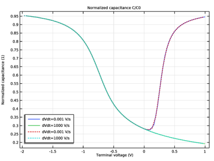
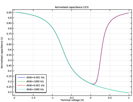
Click to expand the Coloring and Style section. Find the Line style subsection. From the Line list, choose Dotted.
10
From the Width list, choose 2.
11
In the Normalized capacitance C/C0 toolbar, click  Plot.