|
|
|

|
1
|
|
2
|
|
3
|
Click Add.
|
|
4
|
Click
|
|
5
|
|
6
|
Click
|
|
1
|
|
2
|
|
3
|
|
1
|
|
2
|
|
1
|
|
2
|
|
3
|
|
4
|
|
5
|
|
6
|
|
7
|
|
1
|
|
2
|
|
3
|
|
4
|
|
5
|
|
6
|
|
1
|
|
2
|
|
3
|
|
4
|
On the object blk2, select Boundary 4 only.
|
|
5
|
|
1
|
|
2
|
|
3
|
|
4
|
|
5
|
|
6
|
|
1
|
|
2
|
|
3
|
|
4
|
|
5
|
|
6
|
|
1
|
|
2
|
|
3
|
|
4
|
|
5
|
|
1
|
|
2
|
|
3
|
|
4
|
|
1
|
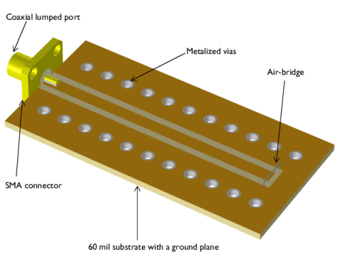
In the Model Builder window, under Component 1 (comp1)>Geometry 1 click SMA Connector, Square Flange with Four Holes 1 (pi1).
|
|
2
|
|
3
|
|
4
|
|
5
|
|
6
|
|
7
|
|
8
|
|
1
|
|
2
|
|
3
|
|
4
|
|
5
|
|
1
|
|
2
|
Select the object cyl1 only.
|
|
3
|
|
4
|
|
5
|
|
6
|
|
7
|
|
1
|
|
2
|
|
3
|
|
4
|
|
5
|
Select the objects arr1(1,1,1), arr1(1,2,1), arr1(10,1,1), arr1(10,2,1), arr1(11,1,1), arr1(11,2,1), arr1(2,1,1), arr1(2,2,1), arr1(3,1,1), arr1(3,2,1), arr1(4,1,1), arr1(4,2,1), arr1(5,1,1), arr1(5,2,1), arr1(6,1,1), arr1(6,2,1), arr1(7,1,1), arr1(7,2,1), arr1(8,1,1), arr1(8,2,1), arr1(9,1,1), and arr1(9,2,1) only.
|
|
6
|
|
1
|
|
2
|
|
3
|
|
4
|
|
5
|
|
1
|
|
2
|
|
3
|
|
4
|
|
5
|
|
1
|
|
2
|
|
3
|
|
4
|
|
5
|
|
6
|
|
1
|
|
2
|
Select the object r2 only.
|
|
3
|
|
4
|
|
5
|
Select the object r1 only.
|
|
1
|
|
2
|
|
3
|
|
4
|
|
5
|
|
6
|
|
1
|
In the Model Builder window, under Component 1 (comp1) right-click Electromagnetic Waves, Frequency Domain (emw) and choose the boundary condition Perfect Electric Conductor.
|
|
2
|
|
3
|
|
4
|
|
5
|
Click OK.
|
|
1
|
|
2
|
|
3
|
From the Selection list, choose Conductive surface (SMA Connector, Square Flange with Four Holes 1).
|
|
1
|
|
3
|
|
4
|
|
1
|
|
1
|
|
1
|
In the Model Builder window, under Component 1 (comp1) right-click Materials and choose Blank Material.
|
|
2
|
|
1
|
|
2
|
|
3
|
|
4
|
|
1
|
|
3
|
|
1
|
|
2
|
|
3
|
|
4
|
|
1
|
|
2
|
|
3
|
|
4
|
|
5
|
|
6
|
|
7
|
|
8
|
|
9
|
|
10
|
|
11
|
Click OK.
|
|
12
|
|
1
|
|
2
|
Right-click Component 1 (comp1)>Electromagnetic Waves, Frequency Domain (emw) and choose the boundary condition Perfect Electric Conductor.
|
|
1
|
|
2
|
|
3
|
|
1
|
In the Model Builder window, under Component 1 (comp1)>Electromagnetic Waves, Frequency Domain (emw) click Perfect Electric Conductor 2.
|
|
1
|
|
2
|
|
3
|
|
5
|
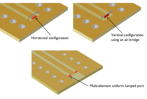
Locate the Lumped Port Properties section. From the Type of lumped port list, choose Multielement uniform.
|
|
1
|
|
2
|
|
3
|
|
5
|
|
1
|
|
3
|
|
4
|
|
1
|
In the Model Builder window, under Component 1 (comp1)>Electromagnetic Waves, Frequency Domain (emw) right-click Perfect Electric Conductor 4 and choose Disable.
|
|
2
|
|
1
|
|
2
|
|
1
|
In the Model Builder window, under Results>Electric Field (emw) right-click Multislice and choose Disable.
|
|
1
|
|
2
|
|
3
|
From the Selection list, choose Conductive surface (SMA Connector, Square Flange with Four Holes 1).
|
|
1
|
|
2
|
|
3
|
|
4
|
|
5
|
Click OK.
|
|
6
|
|
7
|
|
1
|
|
2
|
|
3
|
|
1
|
|
2
|
|
3
|
|
4
|
|
5
|
Click OK.
|
|
1
|
|
3
|