PDF

Balanced Patch Antenna for 6 GHz
Introduction
Patch antennas are becoming more common in wireless equipment, like wireless LAN access points, cellular phones, and GPS handheld devices. The antennas are small in size and can be manufactured with simple and cost-effective techniques. Due to the complicated relationship between the geometry of the antenna and the electromagnetic fields, it is difficult to estimate the properties of a certain antenna shape. At the early stages of antenna design, engineers can benefit a lot from using computer simulations. The changes in the shape of the patch are directly related to the changes in radiation pattern, antenna efficiency, and antenna impedance.
Balanced antennas are fed using two inputs, resulting in less disturbances on the total system through the ground. Balanced systems also provide a degree of freedom to alter antenna properties, by adjusting the phase and magnitude of the two input signals. Figure 1 shows the antenna that this example simulates.
Figure 1: A photo of the real antenna that the model extracts the properties for.
Model Definition
The patch antenna is fabricated on a printed circuit board (PCB) with a relative dielectric constant of 5.23 (Ref. 1). The entire backside is covered with copper, and the front side has a pattern as shown in Figure 2 below.
Figure 2: The patch antenna. The PCB is has a side length of 50 mm and a thickness of 0.7 mm. The centered printed square is 10 mm by 10 mm, the smaller rectangles are 5.2 mm by 3.8 mm, the thicker lines are 0.6 mm wide, and the thinner lines are 0.2 mm by 5.2 mm.
The coaxial cables have an outer conductor with an inner diameter of 4 mm and a center conductor with a diameter of 1 mm. The gap between the conductors is filled with a material with a dielectric constant of 2.07, giving a characteristic impedance close to 58 Ω. There are two coaxial cables feeding the patch antenna from two sides. In this example, the signals in the cables have the same magnitude but are shifted 180 degrees in phase. This results in a balanced feed.
The entire antenna is modeled in 3D. The time-harmonic nature of the signals makes it possible to solve the vector-Helmholtz equation for the electric field everywhere in the geometry,
where k0 is the wave number for free space and is defined as
All metallic objects are defined as perfect electric conductors. The antenna is placed in a spherical air domain surrounded by a Perfectly Matched Layer (PML) serving to absorb the radiation from the antenna with a minimum of reflection.
The model is run through a range of frequencies surrounding the operational frequency of 6.28 GHz.
Results and Discussion
Figure 3: The patch antenna with the electric field plotted both on its surface and on a slice through the air domain. The surrounding PML is hidden from view.
Figure 3 shows the distribution of the electric field norm on the surface of the antenna and in the air, at 6.26 GHz. Most of the energy radiates out from the central patch.
The Lumped Port boundary condition, which is applied to the coaxial cables, is mimicking a connection to a transmission line feed with a characteristic impedance, Zref. The incident voltage wave from the transmission line has an amplitude equal to V0, part of which is reflected directly at the port depending on how well Zref matches the characteristic impedance of the coaxial cable.
Under these circumstances and from each coaxial cable, the theoretical maximum power that can be produced in the antenna is achieved when the antenna impedance matches that of the coaxial cable. This power evaluates to
where V0 is the peak value of the time-harmonic applied voltage.
The antenna efficiency η is defined as the fraction of the theoretical max power that actually radiates out of the antenna:
where P1 and P2 are the net power flow through ports 1 and 2 respectively. In Figure 4 this efficiency is plotted against the frequency, showing that the optimum operating frequency is located at 6.24 GHz.
Figure 4: The antenna efficiency as a function of the frequency.
Application Library path: RF_Module/Antennas/patch_antenna
Notes About the COMSOL Implementation
Possible model extensions include the addition of an external circuit or a far-field computation.
Reference
1. E. Recht and S. Shiran, “A Simple Model for Characteristic Impedance of Wide Microstrip Lines for Flexible PCB,” Proceedings of IEEE EMC Symposium 2000, pp. 1010–1014, 2000.
Modeling Instructions
From the File menu, choose New.
New
In the New window, click  Model Wizard.
Model Wizard
1
In the Model Wizard window, click  3D.
2
In the Select Physics tree, select Radio Frequency>Electromagnetic Waves, Frequency Domain (emw).
3
Click Add.
4
Click  Study.
5
In the Select Study tree, select General Studies>Frequency Domain.
6
Study 1
Step 1: Frequency Domain
1
In the Model Builder window, under Study 1 click Step 1: Frequency Domain.
2
In the Settings window for Frequency Domain, locate the Study Settings section.
3
In the Frequencies text field, type range(6.2[GHz], 0.02[GHz], 6.3[GHz]).
Global Definitions
Parameters 1
1
In the Model Builder window, under Global Definitions click Parameters 1.
2
In the Settings window for Parameters, locate the Parameters section.
3
Geometry 1
Import 1 (imp1)
1
In the Home toolbar, click  Import.
2
In the Settings window for Import, locate the Import section.
3
Click  Browse.
4
5
Click  Import.
The imported geometry consists of the patch antenna and its connectors. Add two concentric spheres, one for the air surrounding the antenna and one for the PML.
Sphere 1 (sph1)
1
In the Geometry toolbar, click  Sphere.
2
In the Settings window for Sphere, locate the Size section.
3
In the Radius text field, type 0.06.
4
Click to expand the Layers section. In the table, enter the following settings:
5
Click  Build All Objects.
6
Click the  Wireframe Rendering button in the Graphics toolbar.
7
Click the  Zoom Extents button in the Graphics toolbar.
Definitions
Perfectly Matched Layer 1 (pml1)
1
In the Definitions toolbar, click  Perfectly Matched Layer.
Activate the PML in the volume covered by the outer but not the inner sphere:
2
3
In the Settings window for Perfectly Matched Layer, locate the Geometry section.
4
From the Type list, choose Spherical.
Add Material
1
In the Home toolbar, click  Add Material to open the Add Material window.
2
Go to the Add Material window.
3
4
Click Add to Component in the window toolbar.
5
In the Home toolbar, click  Add Material to close the Add Material window.
Materials
Coax Dielectric
1
In the Model Builder window, under Component 1 (comp1) right-click Materials and choose Blank Material.
2
In the Settings window for Material, type Coax Dielectric in the Label text field.
3
Locate the Geometric Entity Selection section. Click  Clear Selection.
Select the cylinders between the inner and outer conductors of the coaxial cables:
4
5
Locate the Material Contents section. In the table, enter the following settings:
PCB
1
Right-click Materials and choose Blank Material.
2
In the Settings window for Material, type PCB in the Label text field.
Select the PCB board:
3
4
Locate the Material Contents section. In the table, enter the following settings:
Electromagnetic Waves, Frequency Domain (emw)
By default, the Electromagnetic Waves equation is active in all domains. However, because you represent the metal in this model as perfectly conductive boundaries, there is no need to model the interior of the contacts. Therefore, remove the metal domains from the domains selection.
1
In the Model Builder window, under Component 1 (comp1) click Electromagnetic Waves, Frequency Domain (emw).
2
In the Settings window for Electromagnetic Waves, Frequency Domain, locate the Domain Selection section.
3
Click  Clear Selection.
4
Click  Paste Selection.
5
In the Paste Selection dialog box, type 1-5, 7, 9, 11, 13-16 in the Selection text field.
6
Lumped Port 1
1
In the Physics toolbar, click  Boundaries and choose Lumped Port.
To define the first port, select the outer air/dielectric boundary on the cable facing the x direction:
2
3
In the Settings window for Lumped Port, locate the Lumped Port Properties section.
4
From the Type of lumped port list, choose Coaxial.
For the first port, wave excitation is on by default.
5
Locate the Settings section. In the V0 text field, type V0.
6
In the Zref text field, type Z_coax.
Lumped Port 2
1
In the Physics toolbar, click  Boundaries and choose Lumped Port.
The second port is the outer air/dielectric boundary on the contact facing the y direction:
2
3
In the Settings window for Lumped Port, locate the Lumped Port Properties section.
4
From the Type of lumped port list, choose Coaxial.
5
From the Wave excitation at this port list, choose On.
6
Locate the Settings section. In the V0 text field, type V0.
7
In the θin text field, type pi.
8
In the Zref text field, type Z_coax.
Although you have not yet specified any conducting boundaries, there is already a Perfect Electric Conductor condition in the model. By default, it applies to all boundaries that are exterior to the active domains. It then gets overridden by any other conditions that you are applying. If you click its node in the Model Builder, you can see that it still applies to the conductors.
Perfect Electric Conductor 1
The patch and the PCB ground plane are interior to the model domain (meaning they neighbor only to domains where the equation is active) and hence need to be explicitly assigned this same condition.
Perfect Electric Conductor 2
1
In the Physics toolbar, click  Boundaries and choose Perfect Electric Conductor.
Select the patch and the ground plane (bottom surface) of the PCB:
2
The settings that you have made until now completely define the physics of your model. To enable postprocessing of the antenna efficiency, you need to add integral operators on the port boundaries.
Definitions
Variables 1
1
In the Home toolbar, click  Variables and choose Local Variables.
2
In the Settings window for Variables, locate the Variables section.
3
The power that goes through each of the ports is computed from port voltage and current. The last variable defines the efficiency as the ratio of the input power and the theoretical maximum for each port.
Mesh 1
In the Model Builder window, under Component 1 (comp1) right-click Mesh 1 and choose Build All.
Study 1
In the Home toolbar, click  Compute.
Results
Electric Field (emw)
The default plot shows a slice plot of the electric field norm at 6.3 GHz. It is dominated by the result near the antenna. Most of the remaining part of these model instructions will guide you toward an informative and nice-looking plot of the local electric field on and around the antenna. But first, take the following steps in order to plot the antenna efficiency versus the frequency.
1D Plot Group 2
1
In the Home toolbar, click  Add Plot Group and choose 1D Plot Group.
2
In the Settings window for 1D Plot Group, click to expand the Title section.
3
From the Title type list, choose Manual.
4
In the Title text area, type Efficiency.
5
Locate the Plot Settings section.
6
Select the x-axis label check box. In the associated text field, type Frequency (GHz).
Global 1
1
Right-click 1D Plot Group 2 and choose Global.
2
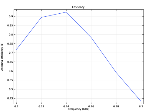
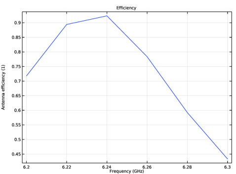
In the Settings window for Global, click Replace Expression in the upper-right corner of the y-Axis Data section. From the menu, choose Component 1 (comp1)>Definitions>Variables>eff - Antenna efficiency.
3
Click to expand the Legends section. Clear the Show legends check box.
4
In the 1D Plot Group 2 toolbar, click  Plot.
The plot has sharp edges because you solved only for 6 frequencies. See Figure 4 for a smoother version over a wider frequency range.
Electric Field (emw)
The plot group you just selected already contains a slice plot of the electric field norm.
Multislice
Delete the multislice plot and add a single slice.
1
In the Model Builder window, expand the Electric Field (emw) node.
2
Right-click Results>Electric Field (emw)>Multislice and choose Delete.
Slice 1
1
In the Model Builder window, right-click Electric Field (emw) and choose Slice.
2
In the Settings window for Slice, locate the Plane Data section.
3
From the Plane list, choose ZX-planes.
4
In the Planes text field, type 1.
5
Click to expand the Range section. Select the Manual color range check box.
6
In the Maximum text field, type 500.
7
Locate the Coloring and Style section. Click  Change Color Table.
8
In the Color Table dialog box, select Thermal>ThermalDark in the tree.
9
Transparency 1
Right-click Slice 1 and choose Transparency.
Selection 1
1
In the Model Builder window, right-click Slice 1 and choose Selection.
2
In the Settings window for Selection, locate the Selection section.
3
Click  Paste Selection.
4
In the Paste Selection dialog box, type 5-12 in the Selection text field.
5
6
In the Electric Field (emw) toolbar, click  Plot.
You are now looking at a nicely scaled plot of the electric field norm on a slice of your geometry, excluding the PML where it does not have any physical relevance.
Surface 1
In the Model Builder window, right-click Electric Field (emw) and choose Surface.
Selection 1
1
In the Model Builder window, right-click Surface 1 and choose Selection.
2
In the Settings window for Selection, locate the Selection section.
3
Click  Paste Selection.
4
In the Paste Selection dialog box, type 13-106, 114-121, 131-144 in the Selection text field.
5
6
In the Electric Field (emw) toolbar, click  Plot.
The electric field norm now also shows up on the surface of the antenna. All exterior surfaces are hidden from view, but the edges defining the contour of the PML are still visible.
Electric Field (emw)
1
In the Model Builder window, under Results click Electric Field (emw).
2
In the Settings window for 3D Plot Group, locate the Plot Settings section.
3
Clear the Plot dataset edges check box.
4
In the Electric Field (emw) toolbar, click  Plot.
Now all edges are gone. This makes the contours of the PCB and the contacts less prominent. To retain a sharper-looking geometry, draw your selected edges in black with the help of a line plot.
Line 1
1
Right-click Electric Field (emw) and choose Line.
2
In the Settings window for Line, locate the Expression section.
3
In the Expression text field, type 1.
4
Locate the Coloring and Style section. From the Coloring list, choose Uniform.
5
From the Color list, choose Black.
Selection 1
1
Right-click Line 1 and choose Selection.
2
In the Settings window for Selection, locate the Selection section.
3
Click  Paste Selection.
4
In the Paste Selection dialog box, type 10-235, 243-264, 278-335 in the Selection text field.
5
6
In the Electric Field (emw) toolbar, click  Plot.
Electric Field (emw)
1
In the Model Builder window, under Results click Electric Field (emw).
2
In the Settings window for 3D Plot Group, click to expand the Title section.
3
From the Title type list, choose Manual.
4
In the Title text area, type Electric field norm (V/m).
5
In the Electric Field (emw) toolbar, click  Plot.
6
Click the  Go to Default View button in the Graphics toolbar.
Your plot should now look like that in Figure 3.