PDF

Monopole Antenna Array
Introduction
It is possible to shape the radiation pattern and steer the beam from an antenna array by controlling the relative phases and magnitudes of the input signal. This example shows how to design an active electronically scanned array (AESA) using arithmetic phase progression on each antenna element.
Figure 1: × 1 monopole antenna array on a substrate.
Model Definition
This example (Figure 1) simulates four quarter-wave monopole antenna mounted on a dielectric substrate. Each antenna is fed by a coaxial lumped port and the outer conductor of each coaxial feed is connected to the ground plane on the bottom of the dielectric (εr = 3.38) substrate. The space between the inner and outer conductor of the coaxial cable is filled with Teflon. The distance between the antenna elements is 0.47 wavelength in free space compromising a relatively high gain and low sidelobes as well as preventing unwanted grating lobes. Metallic circles are patterned on the top of the substrate and connected to the each monopole radiator part. These circular patches compensate the inductance caused by the monopole design and provide a reasonable impedance matching to the reference impedance 50 Ω. All metal parts are modeled as perfect electric conductor (PEC). The antenna is modeled in a spherical air domain. The air domain is truncated with the Perfectly Matched Layers (PMLs) to absorb the radiated fields from the array structure.
All domains except the PMLs are meshed by a tetrahedral mesh with maximum element size of five elements per wavelength so that the wave is well resolved. The monopole radiators and coaxial cables are meshed more finely to provide good resolution of the curved surfaces. The PMLs are swept with a total of five elements along the absorbing direction.
First, only the rightmost antenna element is excited while the rest of elements are terminated with 50 Ω to show a relatively low gain radiation pattern and distortion from the coupling with passive elements. Then, all elements are excited with the same magnitude and arithmetic phase variation (0, α, 2α, 3α) with the unit phase α as in Table 1 to generate a higher gain and scannable radiation pattern.
Results and Discussion
The maximum range of the default electric field norm plot is adjusted to emphasize the near field around the monopole radiators in Figure 2. Though only one antenna is excited, the electric fields coupled to other antenna elements are observed, too. The 3D far-field pattern in Figure 3 is distorted compared to that of a typical monopole antenna due to the coupling and asymmetric ground plane configuration to the excited antenna.
When all antenna elements are excited at the same time (Figure 4), the radiation pattern is more directive. While the unit phase α is parametrically swept from -90 to 90 degrees, the direction of maximum radiation is changing gradually.
Figure 2: The strongest electric fields are observed around the excited monopole antenna. The plot also shows that the excited energy is coupled to other antennas elements.
Figure 3: The distorted radiation pattern is generated due to the coupling to the passive antenna elements.
Figure 4: Each antenna element shows a strong field distribution around the monopole radiator.
The direction of maximum radiation is normal to the equiphase plane, so the radiation pattern is tilted to the direction of the faster antenna element in terms of phase. This is the basic idea of a phased array which can steer the beam toward a desired direction; See Figure 5.
Figure 5: 3D far-field radiation pattern while the unit phase variation is changing from -90 to 90 degrees in 45  degree steps.
Application Library path: RF_Module/Antenna_Arrays/monopole_antenna_array
Modeling Instructions
From the File menu, choose New.
New
In the New window, click  Model Wizard.
Model Wizard
1
In the Model Wizard window, click  3D.
2
In the Select Physics tree, select Radio Frequency>Electromagnetic Waves, Frequency Domain (emw).
3
Click Add.
4
Click  Study.
5
In the Select Study tree, select General Studies>Frequency Domain.
6
Study 1
Step 1: Frequency Domain
1
In the Model Builder window, under Study 1 click Step 1: Frequency Domain.
2
In the Settings window for Frequency Domain, locate the Study Settings section.
3
In the Frequencies text field, type 2.4[GHz].
Global Definitions
Parameters 1
1
In the Model Builder window, under Global Definitions click Parameters 1.
2
In the Settings window for Parameters, locate the Parameters section.
3
Here, c_const is a predefined COMSOL constant for the speed of light in vacuum.
Geometry 1
1
In the Model Builder window, under Component 1 (comp1) click Geometry 1.
2
In the Settings window for Geometry, locate the Units section.
3
From the Length unit list, choose mm.
Sphere 1 (sph1)
1
In the Geometry toolbar, click  Sphere.
2
In the Settings window for Sphere, locate the Size section.
3
In the Radius text field, type 180.
4
Click to expand the Layers section. In the table, enter the following settings:
Block 1 (blk1)
1
In the Geometry toolbar, click  Block.
2
Click the  Wireframe Rendering button in the Graphics toolbar.
3
In the Settings window for Block, locate the Size and Shape section.
4
In the Width text field, type 60.
5
In the Depth text field, type 240.
6
In the Height text field, type 5.
7
Locate the Position section. In the x text field, type -30.
8
In the y text field, type -120.
Cylinder 1 (cyl1)
1
In the Geometry toolbar, click  Cylinder.
2
In the Settings window for Cylinder, locate the Size and Shape section.
3
In the Radius text field, type 0.5.
4
In the Height text field, type 41.
5
Locate the Position section. In the y text field, type -1.5*spacing.
6
In the z text field, type -5.
Cylinder 2 (cyl2)
1
In the Geometry toolbar, click  Cylinder.
2
In the Settings window for Cylinder, locate the Size and Shape section.
3
In the Radius text field, type 2.35.
4
In the Height text field, type 5.
5
Locate the Position section. In the y text field, type -1.5*spacing.
6
In the z text field, type -5.
Work Plane 1 (wp1)
1
In the Geometry toolbar, click  Work Plane.
2
In the Settings window for Work Plane, locate the Plane Definition section.
3
In the z-coordinate text field, type 5.
4
Click  Show Work Plane.
Work Plane 1 (wp1)>Circle 1 (c1)
1
In the Work Plane toolbar, click  Circle.
2
In the Settings window for Circle, locate the Size and Shape section.
3
In the Radius text field, type 5.5.
4
Locate the Position section. In the yw text field, type -1.5*spacing.
Array 1 (arr1)
1
In the Model Builder window, right-click Geometry 1 and choose Transforms>Array.
2
Select the objects cyl1, cyl2, and wp1 only.
3
In the Settings window for Array, locate the Size section.
4
In the y size text field, type 4.
5
Locate the Displacement section. In the y text field, type spacing.
6
Click  Build All Objects.
The finished geometry should look like this.
Definitions
Perfectly Matched Layer 1 (pml1)
1
In the Definitions toolbar, click  Perfectly Matched Layer.
2
3
In the Settings window for Perfectly Matched Layer, locate the Geometry section.
4
From the Type list, choose Spherical.
Electromagnetic Waves, Frequency Domain (emw)
1
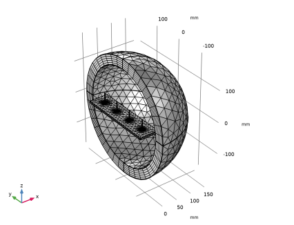
In the Model Builder window, under Component 1 (comp1) click Electromagnetic Waves, Frequency Domain (emw).
2
These are all domains except the monopole radiators and center conductor of the coaxial feeds. By removing from the model domain, PEC conditions are applied by default on the boundaries of the removed domains.
Perfect Electric Conductor 2
1
In the Physics toolbar, click  Boundaries and choose Perfect Electric Conductor.
2
You can do this most easily by copying the text ’15, 18–23, 26, 27, 30, 31, 34, 35, 85, 92, 93, 100, 109, 116, 117, and 124’, clicking in the selection box, and then pressing Ctrl+V, or by using the Paste Selection dialog box.
Lumped Port 1
1
In the Physics toolbar, click  Boundaries and choose Lumped Port.
2
3
In the Settings window for Lumped Port, locate the Lumped Port Properties section.
4
From the Type of lumped port list, choose Coaxial.
For the first port, wave excitation is on by default.
5
Click the  Zoom Extents button in the Graphics toolbar.
Far-Field Domain 1
In the Physics toolbar, click  Domains and choose Far-Field Domain.
Add Material
1
In the Home toolbar, click  Add Material to open the Add Material window.
2
Go to the Add Material window.
3
4
Click Add to Component in the window toolbar.
5
In the Home toolbar, click  Add Material to close the Add Material window.
Materials
Material 2 (mat2)
1
In the Model Builder window, under Component 1 (comp1) right-click Materials and choose Blank Material.
2
3
In the Settings window for Material, locate the Material Contents section.
4
Material 3 (mat3)
1
Right-click Materials and choose Blank Material.
2
3
In the Settings window for Material, locate the Material Contents section.
4
Mesh 1
In the Model Builder window, under Component 1 (comp1) right-click Mesh 1 and choose Build All.
Definitions
Hide for Physics 1
1
In the Model Builder window, right-click View 1 and choose Hide for Physics.
2
Hide for Physics 2
1
Right-click View 1 and choose Hide for Physics.
2
In the Settings window for Hide for Physics, locate the Geometric Entity Selection section.
3
From the Geometric entity level list, choose Boundary.
4
Mesh 1
Click the  Zoom In button in the Graphics toolbar.
Study 1
In the Home toolbar, click  Compute.
Results
S-parameter (emw)
S-parameter is calculated with a single port excitation. When the antenna is matched properly, the computed S-parameter value (S11) should be better than -10dB.
1
In the Model Builder window, expand the Results>Derived Values node.
Multislice
1
In the Model Builder window, expand the Results>Electric Field (emw) node, then click Multislice.
2
In the Settings window for Multislice, locate the Expression section.
3
In the Expression text field, type 20*log10(emw.normE).
4
Locate the Multiplane Data section. Find the Y-planes subsection. In the Planes text field, type 0.
5
Find the Z-planes subsection. In the Planes text field, type 0.
6
Find the X-planes subsection. From the Entry method list, choose Coordinates.
7
In the Coordinates text field, type 0.
8
In the Electric Field (emw) toolbar, click  Plot.
9
Click to expand the Range section. Select the Manual color range check box.
10
In the Minimum text field, type 0.
11
In the Electric Field (emw) toolbar, click  Plot.
12
Click the  Zoom Extents button in the Graphics toolbar.
13
Click the  Zoom In button in the Graphics toolbar.
Compare the reproduced plot with Figure 2.
Radiation Pattern 1
1
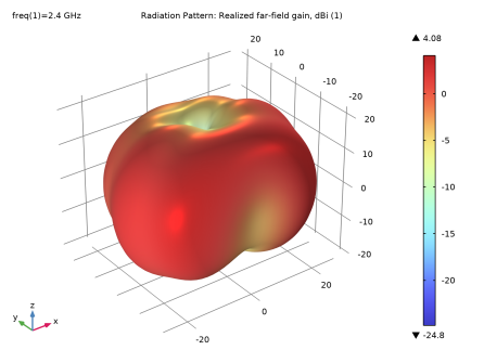
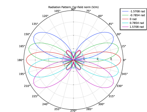
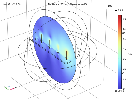
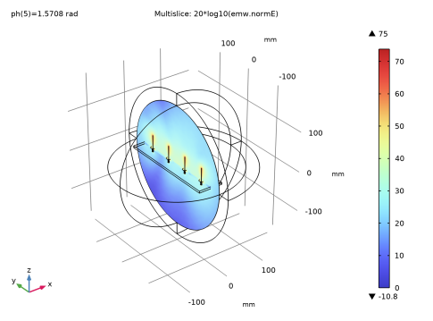
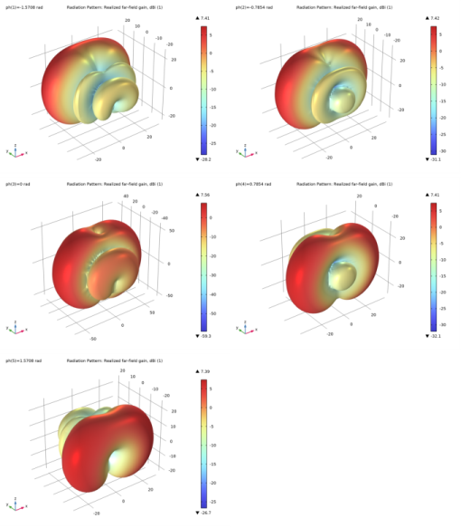
In the Model Builder window, expand the 3D Far Field, Gain (emw) node, then click Radiation Pattern 1.
2
In the Settings window for Radiation Pattern, locate the Evaluation section.
3
Find the Angles subsection. In the Number of elevation angles text field, type 90.
4
In the Number of azimuth angles text field, type 90.
5
In the 3D Far Field, Gain (emw) toolbar, click  Plot.
Table
1
Go to the Table window.
This reproduces Figure 3.
Excite all ports with arithmetic phase variation using the parameter ph defined previously.
Electromagnetic Waves, Frequency Domain (emw)
Lumped Port 2
1
In the Physics toolbar, click  Boundaries and choose Lumped Port.
2
Click the  Zoom Extents button in the Graphics toolbar.
3
4
In the Settings window for Lumped Port, locate the Lumped Port Properties section.
5
From the Type of lumped port list, choose Coaxial.
6
From the Wave excitation at this port list, choose On.
7
Locate the Settings section. In the θin text field, type ph.
Lumped Port 3
1
In the Physics toolbar, click  Boundaries and choose Lumped Port.
2
3
In the Settings window for Lumped Port, locate the Lumped Port Properties section.
4
From the Type of lumped port list, choose Coaxial.
5
From the Wave excitation at this port list, choose On.
6
Locate the Settings section. In the θin text field, type ph*2.
Lumped Port 4
1
In the Physics toolbar, click  Boundaries and choose Lumped Port.
2
3
In the Settings window for Lumped Port, locate the Lumped Port Properties section.
4
From the Type of lumped port list, choose Coaxial.
5
From the Wave excitation at this port list, choose On.
6
Locate the Settings section. In the θin text field, type ph*3.
Study 1
Parametric Sweep
1
In the Study toolbar, click  Parametric Sweep.
2
In the Settings window for Parametric Sweep, locate the Study Settings section.
3
4
From the list in the Parameter name column, choose ph (Array phase progression).
5
Click  Range.
6
In the Range dialog box, type -90[deg] in the Start text field.
7
In the Step text field, type 45[deg].
8
In the Stop text field, type 90[deg].
9
Click Add.
Results
S-parameter (emw)
In the Model Builder window, under Results>Derived Values right-click S-parameter (emw) and choose Disable, as for multiple port excitation the S-parameter is not defined.
Study 1
In the Study toolbar, click  Compute.
Results
Radiation Pattern 1
1
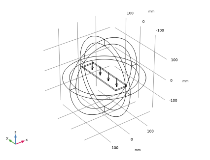
In the Model Builder window, expand the Results>2D Far Field (emw) node, then click Radiation Pattern 1.
2
In the 2D Far Field (emw) toolbar, click  Plot.
3D Far Field, Gain (emw)
1
Click the  Zoom Extents button in the Graphics toolbar.
2
In the Model Builder window, under Results click 3D Far Field, Gain (emw).
3
In the Settings window for 3D Plot Group, locate the Data section.
4
From the Parameter value (ph (rad)) list, choose -0.7854.
5
In the 3D Far Field, Gain (emw) toolbar, click  Plot.
6
From the Parameter value (ph (rad)) list, choose 0.
7
In the 3D Far Field, Gain (emw) toolbar, click  Plot.
8
From the Parameter value (ph (rad)) list, choose 0.7854.
9
In the 3D Far Field, Gain (emw) toolbar, click  Plot.
10
From the Parameter value (ph (rad)) list, choose 1.5708.
11
In the 3D Far Field, Gain (emw) toolbar, click  Plot.
Compare the plotted each 3D radiation pattern with Figure 5.