PDF

Feasibility Study of Microstrip Patch Antenna Array Design
Introduction
An antenna array is a group of radiators or array of antenna elements. By controlling the phase and magnitude of the input signal assigned on each antenna element, as well as the number and arrangement of elements in the array, it is possible to steer the radiation pattern in a desired direction with a preferred level of gain. In this example, a 4 ? 2 array of patch antennas is fed from a single feed point, with all elements fed at equal phase and magnitude.
Figure 1: A 4 2 slot coupled microstrip patch antenna array. The model consists of a PEC ground plane, a feed network for uniform distribution excited by a lumped port beneath the ground plane, with slot coupled rectangular patch antennas above the ground plane. A perfectly matched layer domain truncates the region of free space around the antenna.
Model Definition
As the number of elements in an antenna array increases, the feed network gets more complicated. Thus, it is desirable to isolate the feed network structure from the antenna structure. In this example, the feed network and the antenna elements are placed on opposite sides of a ground plane, which allows for greater flexibility in the design.
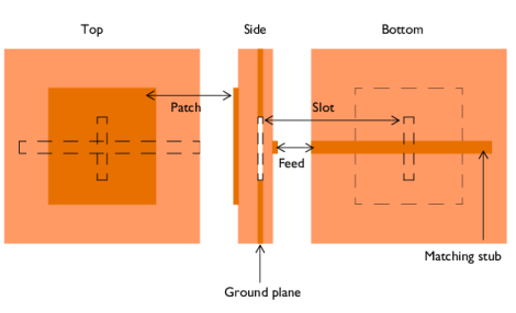
A slot coupled microstrip patch antenna as shown in Figure 2 is used as the radiating element of the array. A thin conducting patch on a substrate sits above a ground plane. A slot in the ground plane is aligned with the center of the antenna. The feed network sits below the ground plane, a 50 Ω microstrip line crosses over the slot, and extends some distance beyond, forming a matching stub. The antenna input impedance is optimized to minimize S11, the reflected power by adjusting the size of the slot and the length of the matching stub.
Figure 2: Slot coupled microstrip patch antenna.
The array antenna consists of a 4 ? 2 rectangular arrangement of equivalent patch antenna elements. The spacing is slightly less than one-half wavelength in free space to avoid a grating lobe and to realize more gain.
The feed network, on the opposite side of the ground plane, is designed to feed each antenna element at the same phase and magnitude. A single feed point, at the center, represents a connection to a 50 Ω transmission line.
Quarter-wave transformers and T-junctions are used to form the 4 ? 2 feed network that distributes the input power uniformly into each antenna element. Two parallel 50 Ω lines combined with a T-junction lower the input impedance and a quarter-wave transformer after the T-junction adjusts the input impedance back to 50 Ω. This design process is repeated until the end of a line reaches the single feed point. The layout on each layer is shown in Figure 3.
Figure 3: The view on each side of the 4 ?2 slot coupled microstrip patch antenna array.
Results and Discussion
The results show that the S11 is better than 10 dB and the front-back ratio in the radiation pattern is more than 20 dB. In Figure 4, the E-plane is defined with the direction of the antenna polarization and includes the direction of a maximum radiation. The H-plane is the plane perpendicular to the direction of the antenna polarization. Since the number of the antenna elements in the H-plane direction is more than in the E-plane direction, the radiation pattern in the H-plane is narrower than the radiation pattern on the E-plane and 12 dB sidelobes are observed only in the H-plane.
Figure 4: Far-field radiation pattern in the E-plane (blue) and the H-plane (green) at 1.68 GHz. The radiation pattern is much more directive than that of a patch antenna.
Figure 5: 3D far-field realized gain pattern is directed toward the top side of the antenna array.
Notes About the COMSOL Implementation
The goal of this example is to do a feasibility study of microstrip patch antenna design. The mesh settings are adjusted to reduce the size of the problem. However, it is still a memory-intensive simulation and may require more than 6 GB RAM.
References
1. D.M. Pozar, Microwave Engineering, John Wiley & Sons, 1998.
2. C.A. Balanis, Antenna Theory, John Wiley & Sons, 1997.
3. R.E. Collin, Antennas and Radiowave Propagation, McGraw-Hill, 1985.
Application Library path: RF_Module/Antenna_Arrays/microstrip_patch_antenna_array
Modeling Instructions
From the File menu, choose New.
New
In the New window, click  Model Wizard.
Model Wizard
1
In the Model Wizard window, click  3D.
2
In the Select Physics tree, select Radio Frequency>Electromagnetic Waves, Frequency Domain (emw).
3
Click Add.
4
Click  Study.
5
In the Select Study tree, select General Studies>Frequency Domain.
6
Global Definitions
Parameters 1
1
In the Model Builder window, under Global Definitions click Parameters 1.
2
In the Settings window for Parameters, locate the Parameters section.
3
Here, c_const is a predefined COMSOL constant for the speed of light in vacuum.
Geometry 1
First, import the microstrip patch antenna array design.
Import 1 (imp1)
1
In the Home toolbar, click  Import.
2
In the Settings window for Import, locate the Import section.
3
Click  Browse.
4
5
Click  Import.
Choose wireframe rendering to get a better view of the interior parts.
6
Click the  Wireframe Rendering button in the Graphics toolbar.
Add a sphere for the perfectly matched layers. Use a layer definition to create shell-type sphere structure.
PML
1
In the Geometry toolbar, click  Sphere.
2
In the Settings window for Sphere, type PML in the Label text field.
3
Locate the Size section. In the Radius text field, type 0.275.
4
Click to expand the Layers section. In the table, enter the following settings:
5
Click  Build All Objects.
Definitions
Create a set of selections for use when setting up the physics. First, create a selection for the patch antennas.
Patch
1
In the Definitions toolbar, click  Explicit.
2
In the Settings window for Explicit, type Patch in the Label text field.
3
Locate the Input Entities section. From the Geometric entity level list, choose Boundary.
4
Add selections for the feed network, slot, ground, and substrate.
Feed network
1
In the Definitions toolbar, click  Explicit.
2
In the Settings window for Explicit, type Feed network in the Label text field.
3
Locate the Input Entities section. From the Geometric entity level list, choose Boundary.
4
Slot
1
In the Definitions toolbar, click  Explicit.
2
In the Settings window for Explicit, type Slot in the Label text field.
3
Locate the Input Entities section. From the Geometric entity level list, choose Boundary.
4
Ground
1
In the Definitions toolbar, click  Explicit.
2
In the Settings window for Explicit, type Ground in the Label text field.
3
Locate the Input Entities section. From the Geometric entity level list, choose Boundary.
4
Substrate
1
In the Definitions toolbar, click  Explicit.
2
In the Settings window for Explicit, type Substrate in the Label text field.
3
Zoom out to get a view of the entire structure.
4
Click the  Zoom Out button in the Graphics toolbar.
Perfectly Matched Layer 1 (pml1)
1
In the Definitions toolbar, click  Perfectly Matched Layer.
2
3
In the Settings window for Perfectly Matched Layer, locate the Geometry section.
4
From the Type list, choose Spherical.
Definitions
To get a better view, suppress some of the domains. Furthermore, by assigning the resulting settings to a View node, you can easily return to the same view later by clicking the Go to View 2 button in the Graphics toolbar.
View 2
1
In the Model Builder window, under Component 1 (comp1) right-click Definitions and choose View.
2
Click the  Wireframe Rendering button in the Graphics toolbar.
Hide for Physics 1
1
In the Model Builder window, right-click View 2 and choose Hide for Physics.
2
Hide for Physics 2
1
In the Model Builder window, right-click View 2 and choose Hide for Physics.
2
In the Settings window for Hide for Physics, locate the Geometric Entity Selection section.
3
From the Geometric entity level list, choose Boundary.
4
Electromagnetic Waves, Frequency Domain (emw)
Perfect Electric Conductor 2
1
In the Model Builder window, under Component 1 (comp1) right-click Electromagnetic Waves, Frequency Domain (emw) and choose the boundary condition Perfect Electric Conductor.
2
In the Settings window for Perfect Electric Conductor, locate the Boundary Selection section.
3
From the Selection list, choose Patch.
Perfect Electric Conductor 3
1
In the Physics toolbar, click  Boundaries and choose Perfect Electric Conductor.
2
In the Settings window for Perfect Electric Conductor, locate the Boundary Selection section.
3
From the Selection list, choose Feed network.
Perfect Electric Conductor 4
1
In the Physics toolbar, click  Boundaries and choose Perfect Electric Conductor.
2
In the Settings window for Perfect Electric Conductor, locate the Boundary Selection section.
3
From the Selection list, choose Ground.
Lumped Port 1
1
In the Physics toolbar, click  Boundaries and choose Lumped Port.
2
Click the  Zoom In button in the Graphics toolbar, a couple of times to see the port boundary clearly.
3
For the first port, wave excitation is on by default.
4
Click the  Zoom Extents button in the Graphics toolbar.
Far-Field Domain 1
In the Physics toolbar, click  Domains and choose Far-Field Domain.
Materials
Next, assign material properties to the model. Begin by specifying air for all domains.
Add Material
1
In the Home toolbar, click  Add Material to open the Add Material window.
2
Go to the Add Material window.
3
4
Click Add to Component in the window toolbar.
5
In the Home toolbar, click  Add Material to close the Add Material window.
Materials
Override the substrate with the dielectric material of εrr = 3.38.
Substrate
1
In the Model Builder window, under Component 1 (comp1) right-click Materials and choose Blank Material.
2
In the Settings window for Material, type Substrate in the Label text field.
3
Locate the Geometric Entity Selection section. From the Selection list, choose Substrate.
4
Locate the Material Contents section. In the table, enter the following settings:
Mesh 1
Choose the maximum mesh size in the air domain smaller than 0.2 wavelengths using the parameter h_max that you defined earlier. Scale the mesh size inside the substrate by the inverse of the square root of the relative dielectric constant of the substrate.
Size 1
1
In the Model Builder window, under Component 1 (comp1) right-click Mesh 1 and choose Size.
2
In the Settings window for Size, locate the Element Size section.
3
Click the Custom button.
4
Locate the Element Size Parameters section.
5
Select the Maximum element size check box. In the associated text field, type h_max.
6
Select the Maximum element growth rate check box. In the associated text field, type 2.5.
Due to the thin substrate, use a smaller value for the maximum mesh size than that initially suggested.
Size 2
1
In the Model Builder window, right-click Mesh 1 and choose Size.
2
In the Settings window for Size, locate the Geometric Entity Selection section.
3
From the Geometric entity level list, choose Domain.
4
From the Selection list, choose Substrate.
5
Locate the Element Size section. Click the Custom button.
6
Locate the Element Size Parameters section.
7
Select the Maximum element size check box. In the associated text field, type h_max/sqrt(3.38)/2.
To resolve the small parts properly, refine the mesh further in each selection of the model.
Size 3
1
Right-click Mesh 1 and choose Size.
2
In the Settings window for Size, locate the Geometric Entity Selection section.
3
From the Geometric entity level list, choose Boundary.
4
From the Selection list, choose Feed network.
5
Locate the Element Size section. Click the Custom button.
6
Locate the Element Size Parameters section.
7
Select the Maximum element size check box. In the associated text field, type 1.8[mm].
8
Select the Minimum element size check box. In the associated text field, type 0.5[mm].
Size 4
1
Right-click Mesh 1 and choose Size.
2
In the Settings window for Size, locate the Geometric Entity Selection section.
3
From the Geometric entity level list, choose Boundary.
4
From the Selection list, choose Slot.
5
Locate the Element Size section. Click the Custom button.
6
Locate the Element Size Parameters section.
7
Select the Maximum element size check box. In the associated text field, type 2[mm].
Size 5
1
Right-click Mesh 1 and choose Size.
2
In the Settings window for Size, locate the Geometric Entity Selection section.
3
From the Geometric entity level list, choose Boundary.
4
From the Selection list, choose Patch.
5
Locate the Element Size section. Click the Custom button.
6
Locate the Element Size Parameters section.
7
Select the Maximum element size check box. In the associated text field, type 2[mm].
Size 6
1
Right-click Mesh 1 and choose Size.
2
In the Settings window for Size, locate the Geometric Entity Selection section.
3
From the Geometric entity level list, choose Boundary.
4
From the Selection list, choose Ground.
5
Locate the Element Size section. Click the Custom button.
6
Locate the Element Size Parameters section.
7
Select the Maximum element size check box. In the associated text field, type 4[mm].
Free Tetrahedral 1
1
In the Mesh toolbar, click  Free Tetrahedral.
2
In the Settings window for Free Tetrahedral, locate the Domain Selection section.
3
From the Geometric entity level list, choose Domain.
4
Use a swept mesh for the PMLs.
Swept 1
In the Mesh toolbar, click  Swept.
Distribution 1
1
Right-click Swept 1 and choose Distribution.
2
Right-click Mesh 1 and choose Build All.
Study 1
Step 1: Frequency Domain
1
In the Model Builder window, under Study 1 click Step 1: Frequency Domain.
2
In the Settings window for Frequency Domain, locate the Study Settings section.
3
In the Frequencies text field, type f0.
4
In the Home toolbar, click  Compute.
Results
Electric Field (emw)
Begin the results analysis by reviewing the plot showing the distribution of the electric field norm.
Multislice
1
In the Model Builder window, expand the Electric Field (emw) node, then click Multislice.
2
In the Settings window for Multislice, locate the Expression section.
3
In the Expression text field, type 20*log10(emw.normE).
4
Locate the Multiplane Data section. Find the X-planes subsection. In the Planes text field, type 0.
5
Find the Y-planes subsection. In the Planes text field, type 0.
6
Find the Z-planes subsection. From the Entry method list, choose Coordinates.
7
In the Coordinates text field, type 1.524[mm].
8
Locate the Coloring and Style section. Click  Change Color Table.
9
In the Color Table dialog box, select Thermal>HeatCameraLight in the tree.
10
Selection 1
1
Right-click Multislice and choose Selection.
2
3
Click the  Zoom to Selection button in the Graphics toolbar.
Deformation 1
1
Right-click Multislice and choose Deformation.
2
In the Settings window for Deformation, locate the Expression section.
3
In the X-component text field, type 0.
4
In the Y-component text field, type 0.
5
In the Z-component text field, type 20*log10(emw.normE).
6
In the Electric Field (emw) toolbar, click  Plot.
Strong electric fields are observed on the radiating edges.
Adjust the polar plot settings to visualize the far-field pattern on the E-plane.
Radiation Pattern 1
1
In the Model Builder window, expand the Results>2D Far Field (emw) node, then click Radiation Pattern 1.
2
In the Settings window for Radiation Pattern, locate the Evaluation section.
3
Find the Reference direction subsection. In the x text field, type 0.
4
In the y text field, type 1.
5
Find the Normal vector subsection. In the x text field, type 1.
6
In the z text field, type 0.
7
Click to expand the Legends section. From the Legends list, choose Manual.
8
9
In the 2D Far Field (emw) toolbar, click  Plot.
The E-plane in this model is located on the yz-plane where φ is measured counterclockwise from the y-axis.
Add the H-plane polar plot.
Radiation Pattern 2
1
Right-click Results>2D Far Field (emw)>Radiation Pattern 1 and choose Duplicate.
2
In the Settings window for Radiation Pattern, locate the Evaluation section.
3
Find the Reference direction subsection. In the x text field, type 1.
4
In the y text field, type 0.
5
Find the Normal vector subsection. In the x text field, type 0.
6
In the y text field, type -1.
7
Locate the Legends section. In the table, enter the following settings:
8
In the 2D Far Field (emw) toolbar, click  Plot.
The H-plane is located on the xz-plane where φ is measured counterclockwise from the x-axis.
Compare the resulting plot with that shown in Figure 4.
Radiation Pattern 1
1
In the Model Builder window, expand the 3D Far Field, Gain (emw) node, then click Radiation Pattern 1.
2
In the Settings window for Radiation Pattern, locate the Evaluation section.
3
Find the Angles subsection. In the Number of elevation angles text field, type 90.
4
In the Number of azimuth angles text field, type 90.
5
Locate the Coloring and Style section. Click  Change Color Table.
6
In the Color Table dialog box, select Wave>DiscoLight in the tree.
7
8
In the 3D Far Field, Gain (emw) toolbar, click  Plot.
Table
1
Go to the Table window.
Compare the 3D far-field realized gain pattern plot with Figure 5.
Results
Finish by inspecting the input matching characteristic of the antenna array.