PDF

Modeling of Microstrip Lines with Vias
Introduction
There are multiple ways to excite and terminate transmission lines using different types of port and lumped port features. In this example, transverse electromagnetic (TEM) type ports and a via type lumped port are used to simulate two adjacent microstrip lines. One via end is terminated as a metalized via while the other via end is probing an inflow signal. The computed S-parameters show the amount of crosstalk between the lines and the strength of the signal coupled through the cylindrical via.
Figure 1: Microstrip line circuit board modeled with TEM ports and a via type lumped port. The top air domain is not included for visualization purposes.
Model Definition
The model describes two 50 Ω microstrip lines adjacent to each other on a 60 mil substrate with the dielectric constant of εr = 3.38. One microstrip line is terminated with a via type lumped port and the other line is finished with a metalized via hole. The interior surfaces of metallic parts, including the patterned line on the top of the substrate and a metalized via, are defined using a transition boundary condition to capture the loss from a finite conductivity. The ground plane is located on the exterior surface of the model domain and characterized by an impedance boundary condition that is also used for modeling lossy conductive boundaries.
A transverse electromagnetic (TEM) type port boundary condition is used on each side of the cuboid model domain touching the microstrip line and ground plane. The TEM type port is completed by adding electric potential and ground subfeatures. The edge of microstrip line top trace on the TEM port boundary is set to electric potential while the edge of ground plane on the TEM port boundary is set to ground. The material above the circuit board is air.
Results and Discussion
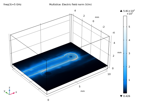
After simulation, the default plot is modified to plot the electric field norm on the top surface of the circuit board as shown in Figure 2. It is observed that the input power to port 1 is partially coupled to the adjacent microstrip line connected to port 3.
Figure 2: Electric field norm plot. A fraction of input power is coupled to the adjacent microstrip line.
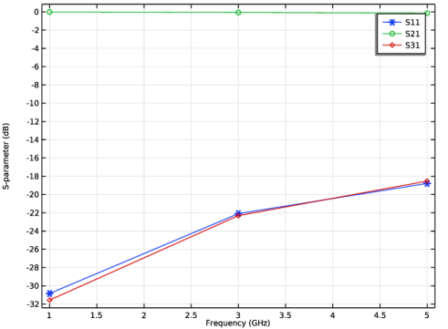
Figure 3 quantitatively shows the amount of coupling and crosstalk among ports. The computed S21 indicates that most of the input power is flown into the via-type lumped port (port 2). The far-end crosstalk in this circuit, S31, increases with the simulation frequency.
Figure 3: S-parameter plot describes impedance mismatching (S11), insertion loss to the via port (S21), and far-end crosstalk, FEXT (S31).
Application Library path: RF_Module/Transmission_Lines_and_Waveguides/microstrip_line_tem_via
Modeling Instructions
From the File menu, choose New.
New
In the New window, click  Model Wizard.
Model Wizard
1
In the Model Wizard window, click  3D.
2
In the Select Physics tree, select Radio Frequency>Electromagnetic Waves, Frequency Domain (emw).
3
Click Add.
4
Click  Study.
5
In the Select Study tree, select Preset Studies for Selected Physics Interfaces>TEM Boundary Mode Analysis.
6
Global Definitions
Parameters 1
1
In the Model Builder window, under Global Definitions click Parameters 1.
2
In the Settings window for Parameters, locate the Parameters section.
3
It is convenient to define parameters for frequently used values. Here, mil refers to the unit milliinch.
Geometry 1
1
In the Model Builder window, under Component 1 (comp1) click Geometry 1.
2
In the Settings window for Geometry, locate the Units section.
3
From the Length unit list, choose mm.
Block 1 (blk1)
1
In the Geometry toolbar, click  Block.
2
In the Settings window for Block, locate the Size and Shape section.
3
In the Width text field, type 10.
4
In the Depth text field, type 8.
5
In the Height text field, type tsub*10.
6
Locate the Position section. In the y text field, type -4.
7
Click to expand the Layers section. In the table, enter the following settings:
Work Plane 1 (wp1)
1
In the Geometry toolbar, click  Work Plane.
Signal traces are patterned on this work plane.
2
In the Settings window for Work Plane, locate the Plane Definition section.
3
In the z-coordinate text field, type tsub.
Work Plane 1 (wp1)>Plane Geometry
In the Model Builder window, click Plane Geometry.
Work Plane 1 (wp1)>Rectangle 1 (r1)
1
In the Work Plane toolbar, click  Rectangle.
2
In the Settings window for Rectangle, locate the Size and Shape section.
3
In the Width text field, type 7.5.
4
In the Height text field, type 1.13.
5
Locate the Position section. In the yw text field, type -0.565+0.8.
Work Plane 1 (wp1)>Circle 1 (c1)
1
In the Work Plane toolbar, click  Circle.
2
In the Settings window for Circle, locate the Size and Shape section.
3
In the Radius text field, type 0.8.
4
Locate the Position section. In the xw text field, type 7.5.
5
In the yw text field, type 0.8.
Work Plane 1 (wp1)>Union 1 (uni1)
1
In the Work Plane toolbar, click  Booleans and Partitions and choose Union.
2
Click in the Graphics window and then press Ctrl+A to select both objects.
3
In the Settings window for Union, locate the Union section.
4
Clear the Keep interior boundaries check box.
5
Click the  Wireframe Rendering button in the Graphics toolbar. The wireframe rendering provides a better view of inside the box.
Cylinder 1 (cyl1)
1
In the Geometry toolbar, click  Cylinder.
2
In the Settings window for Cylinder, locate the Size and Shape section.
3
In the Radius text field, type 0.4.
4
In the Height text field, type tsub.
5
Locate the Position section. In the x text field, type 7.5.
6
In the y text field, type 0.8.
The side surfaces of the cylinder will be configured as Via type lumped port and metalized via hole, later.
Rotate 1 (rot1)
1
In the Geometry toolbar, click  Transforms and choose Rotate.
2
Select the objects cyl1 and wp1 only.
3
In the Settings window for Rotate, locate the Input section.
4
Select the Keep input objects check box.
5
Locate the Rotation section. In the Angle text field, type 180.
6
Click  Build All Objects.
7
Locate the Point on Axis of Rotation section. In the x text field, type 5.
8
Click  Build All Objects.
Electromagnetic Waves, Frequency Domain (emw)
Wave Equation, Electric 2
1
In the Model Builder window, under Component 1 (comp1) right-click Electromagnetic Waves, Frequency Domain (emw) and choose Wave Equation, Electric.
2
3
In the Settings window for Wave Equation, Electric, locate the Electric Displacement Field section.
4
From the Electric displacement field model list, choose Loss tangent, dissipation factor.
The material properties for the substrate, that will imported from the RF material library, are defined based on the dielectric constant and loss tangent. It is necessary to choose the right constitutive relation for the substrate domain.
Transition Boundary Condition 1
1
In the Physics toolbar, click  Boundaries and choose Transition Boundary Condition. Lossy conductive surfaces can be modeled using Transition Boundary Condition for interior boundaries.
2
3
In the Settings window for Transition Boundary Condition, locate the Transition Boundary Condition section.
4
In the d text field, type 38[um].
Impedance Boundary Condition 1
1
In the Physics toolbar, click  Boundaries and choose Impedance Boundary Condition. Lossy conductive surfaces can be modeled using Impedance Boundary Condition for exterior boundaries. This can also be looked as geometrically thick conductive volume.
2
Port 1
1
In the Physics toolbar, click  Boundaries and choose Port.
2
3
In the Settings window for Port, locate the Port Properties section.
4
From the Type of port list, choose Transverse electromagnetic (TEM).
Transmission lines supporting the (quasi-) TEM mode can be analyzed with the TEM type port.
Ground 1
1
In the Physics toolbar, click  Attributes and choose Ground.
The exterior edges of the port boundaries are set to ground by default.
Port 1
In the Model Builder window, click Port 1.
Electric Potential 1
1
In the Physics toolbar, click  Attributes and choose Electric Potential.
2
The electric potential edge is assigned on the signal trace.
Lumped Port 1
1
In the Physics toolbar, click  Boundaries and choose Lumped Port.
2
Click the  Select Box button in the Graphics toolbar.
3
4
In the Settings window for Lumped Port, locate the Lumped Port Properties section.
5
From the Type of lumped port list, choose Via.
Port 2
1
In the Physics toolbar, click  Boundaries and choose Port.
2
3
In the Settings window for Port, locate the Port Properties section.
4
From the Type of port list, choose Transverse electromagnetic (TEM).
Ground 1
In the Physics toolbar, click  Attributes and choose Ground.
Port 2
In the Model Builder window, click Port 2.
Electric Potential 1
1
In the Physics toolbar, click  Attributes and choose Electric Potential.
2
Now, make sure that Advanced Physics Options is enabled. Then, set the physics to use the constraint-based port formulation, that works best with TEM-type ports.
3
Click the  Show More Options button in the Model Builder toolbar.
4
In the Show More Options dialog box, select Physics>Advanced Physics Options in the tree.
5
In the tree, select the check box for the node Physics>Advanced Physics Options.
6
7
In the Model Builder window, click Electromagnetic Waves, Frequency Domain (emw).
8
In the Settings window for Electromagnetic Waves, Frequency Domain, click to expand the Port Options section.
9
From the Port formulation list, choose Constraint-based.
Add Material
1
In the Home toolbar, click  Add Material to open the Add Material window.
2
Go to the Add Material window.
3
4
Click Add to Component in the window toolbar.
5
In the tree, select Built-in>Copper.
6
Click Add to Component in the window toolbar.
Materials
Copper (mat2)
1
In the Settings window for Material, locate the Geometric Entity Selection section.
2
From the Geometric entity level list, choose Boundary.
3
Add Material
1
Go to the Add Material window.
2
In the tree, select RF>Rogers Corporation>Rogers RO4000® Laminates>RO4003C Laminates.
3
Click Add to Component in the window toolbar.
4
In the Home toolbar, click  Add Material to close the Add Material window.
Materials
RO4003C Laminates (mat3)
Select Domain 1 only.
Study 1
Step 2: Frequency Domain
1
In the Model Builder window, under Study 1 click Step 2: Frequency Domain.
2
In the Settings window for Frequency Domain, locate the Study Settings section.
3
In the Frequencies text field, type 1 3 5.
Mesh 1
In the Model Builder window, under Component 1 (comp1) right-click Mesh 1 and choose Build All.
Definitions
View 1
Remove some boundaries from the view to inspect the mesh.
Hide for Physics 1
1
In the Model Builder window, expand the Component 1 (comp1)>Definitions node.
2
Right-click View 1 and choose Hide for Physics.
3
In the Settings window for Hide for Physics, locate the Geometric Entity Selection section.
4
From the Geometric entity level list, choose Boundary.
5
Mesh 1
1
In the Home toolbar, click  Compute.
Results
Multislice
1
In the Model Builder window, expand the Results>Electric Field (emw) node, then click Multislice.
2
In the Settings window for Multislice, locate the Multiplane Data section.
3
Find the X-planes subsection. In the Planes text field, type 0.
4
Find the Y-planes subsection. In the Planes text field, type 0.
5
Find the Z-planes subsection. From the Entry method list, choose Coordinates.
6
In the Coordinates text field, type tsub.
7
Locate the Coloring and Style section. Click  Change Color Table.
8
In the Color Table dialog box, select Aurora>JupiterAuroraBorealis in the tree.
9
Compare the reproduced plot to Figure 2.
Global 1
1
In the Model Builder window, expand the Results>S-parameter (emw) node, then click Global 1.
2
In the Settings window for Global, click to expand the Coloring and Style section.
3
Find the Line markers subsection. From the Marker list, choose Cycle.
The S-parameter plot is shown in Figure 3. This describe the impedance mismatching in the input port and signal coupling to the adjacent microstrip line.
Smith Plot (emw)