|
|
|

|
1
|
|
2
|
|
3
|
Click Add.
|
|
4
|
Click
|
|
5
|
In the Select Study tree, select Preset Studies for Selected Physics Interfaces>TEM Boundary Mode Analysis.
|
|
6
|
Click
|
|
1
|
|
2
|
|
3
|
|
1
|
|
2
|
|
3
|
|
4
|
|
5
|
|
6
|
|
7
|
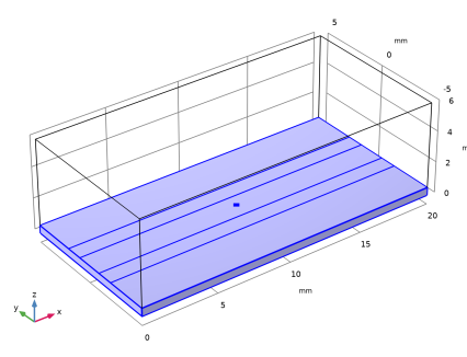
Click to expand the Layers section. In the table, enter the following settings:
|
|
1
|
|
2
|
|
3
|
|
1
|
|
2
|
|
3
|
|
4
|
|
5
|
|
1
|
|
2
|
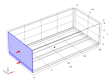
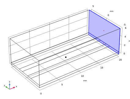
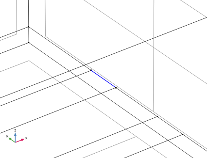
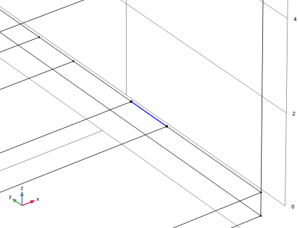
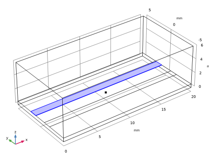
Select the object r1 only.
|
|
3
|
|
4
|
|
5
|
|
6
|
|
1
|
|
2
|
|
3
|
|
4
|
|
5
|
|
6
|
|
1
|
|
2
|
|
3
|
In the tree, select Built-in>Air.
|
|
4
|
|
5
|
|
1
|
In the Model Builder window, under Component 1 (comp1) right-click Materials and choose Blank Material.
|
|
3
|
|
1
|
|
2
|
|
3
|
|
4
|
Click OK.
|
|
5
|
In the Model Builder window, under Component 1 (comp1) click Electromagnetic Waves, Frequency Domain (emw).
|
|
6
|
In the Settings window for Electromagnetic Waves, Frequency Domain, click to expand the Port Options section.
|
|
7
|
|
1
|
|
3
|
|
4
|
|
5
|
|
1
|
|
1
|
|
3
|
|
4
|
|
1
|
|
3
|
|
4
|
|
5
|
|
1
|
|
1
|
|
3
|
|
4
|
|
1
|
|
1
|
|
1
|
|
3
|
|
4
|
|
5
|
|
1
|
In the Model Builder window, under Component 1 (comp1)>Electromagnetic Waves, Frequency Domain (emw) right-click Port 1 and choose Duplicate.
|
|
2
|
|
3
|
|
1
|
|
2
|
Right-click Component 1 (comp1)>Electromagnetic Waves, Frequency Domain (emw)>Port 3>Electric Potential 2 and choose Delete.
|
|
1
|
In the Model Builder window, under Component 1 (comp1)>Electromagnetic Waves, Frequency Domain (emw) right-click Port 2 and choose Duplicate.
|
|
2
|
|
3
|
|
1
|
|
2
|
Right-click Component 1 (comp1)>Electromagnetic Waves, Frequency Domain (emw)>Port 4>Electric Potential 2 and choose Delete.
|
|
1
|
In the Model Builder window, under Component 1 (comp1)>Electromagnetic Waves, Frequency Domain (emw), Ctrl-click to select Port 1 and Port 2.
|
|
2
|
Right-click and choose Group.
|
|
1
|
In the Model Builder window, under Component 1 (comp1)>Electromagnetic Waves, Frequency Domain (emw), Ctrl-click to select Port 3 and Port 4.
|
|
2
|
Right-click and choose Group.
|
|
1
|
|
2
|
|
3
|
|
4
|
|
1
|
|
2
|
|
3
|
|
4
|
|
5
|
|
1
|
|
2
|
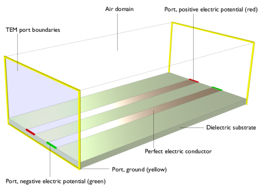
In the Settings window for TEM Boundary Mode Analysis, locate the Physics and Variables Selection section.
|
|
3
|
|
4
|
In the tree, select Component 1 (comp1)>Electromagnetic Waves, Frequency Domain (emw)>Differential Line Port Group.
|
|
5
|
Click
|
|
6
|
In the tree, select Component 1 (comp1)>Electromagnetic Waves, Frequency Domain (emw)>Perfect Electric Conductor 3.
|
|
7
|
Click
|
|
8
|
In the tree, select Component 1 (comp1)>Electromagnetic Waves, Frequency Domain (emw)>Electric Point Dipole 1.
|
|
9
|
Click
|
|
1
|
|
2
|
|
3
|
|
4
|
In the tree, select Component 1 (comp1)>Electromagnetic Waves, Frequency Domain (emw)>Differential Line Port Group.
|
|
5
|
Click
|
|
6
|
In the tree, select Component 1 (comp1)>Electromagnetic Waves, Frequency Domain (emw)>Perfect Electric Conductor 3.
|
|
7
|
Click
|
|
8
|
In the tree, select Component 1 (comp1)>Electromagnetic Waves, Frequency Domain (emw)>Electric Point Dipole 1.
|
|
9
|
Click
|
|
10
|
|
11
|
|
12
|
|
1
|
|
2
|
In the Settings window for Global Evaluation, type S-parameter, Single-Ended Line in the Label text field.
|
|
1
|
|
2
|
In the Settings window for Global Evaluation, type Port Mode Impedance, Single-Ended Line in the Label text field.
|
|
3
|
Click Replace Expression in the upper-right corner of the Expressions section. From the menu, choose Component 1 (comp1)>Electromagnetic Waves, Frequency Domain>TEM boundary mode analysis>emw.Zmode_3 - TEM mode port characteristic impedance - Ω.
|
|
4
|
Click
|
|
1
|
|
2
|
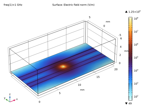
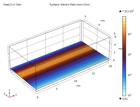
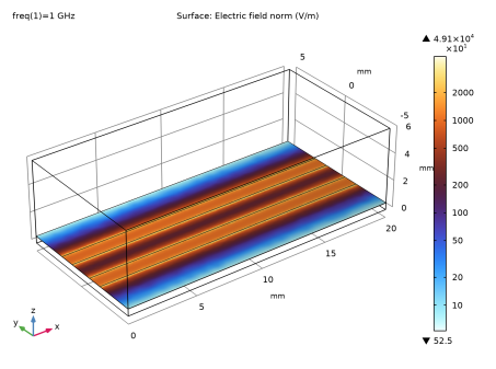
In the Settings window for 3D Plot Group, type Electric Field Norm, Single-Ended Line in the Label text field.
|
|
1
|
|
2
|
|
1
|
|
2
|
|
3
|
|
4
|
|
5
|
Click OK.
|
|
6
|
|
7
|
|
1
|
|
3
|
|
1
|
|
2
|
|
3
|
Find the Studies subsection. In the Select Study tree, select Preset Studies for Selected Physics Interfaces>TEM Boundary Mode Analysis.
|
|
4
|
|
5
|
|
1
|
In the Settings window for TEM Boundary Mode Analysis, locate the Physics and Variables Selection section.
|
|
2
|
|
3
|
In the tree, select Component 1 (comp1)>Electromagnetic Waves, Frequency Domain (emw)>Differential Line Port Group.
|
|
4
|
Right-click and choose Disable.
|
|
5
|
In the tree, select Component 1 (comp1)>Electromagnetic Waves, Frequency Domain (emw)>Perfect Electric Conductor 3.
|
|
6
|
Click
|
|
1
|
|
2
|
|
3
|
|
4
|
In the tree, select Component 1 (comp1)>Electromagnetic Waves, Frequency Domain (emw)>Differential Line Port Group.
|
|
5
|
Right-click and choose Disable.
|
|
6
|
In the tree, select Component 1 (comp1)>Electromagnetic Waves, Frequency Domain (emw)>Perfect Electric Conductor 3.
|
|
7
|
Click
|
|
8
|
|
9
|
In the Settings window for Study, type Study 2, Single-Ended Line with Noise in the Label text field.
|
|
10
|
|
1
|
|
2
|
In the Settings window for Global Evaluation, type S-parameter, Single-Ended Line with Noise in the Label text field.
|
|
1
|
|
2
|
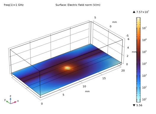
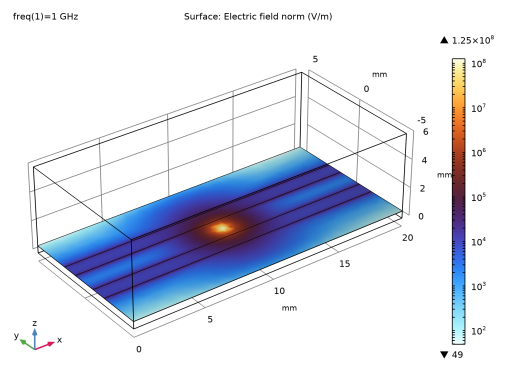
In the Settings window for 3D Plot Group, type Electric Field Norm, Single-Ended Line with Noise in the Label text field.
|
|
1
|
|
2
|
|
1
|
|
2
|
|
3
|
Find the Studies subsection. In the Select Study tree, select Preset Studies for Selected Physics Interfaces>TEM Boundary Mode Analysis.
|
|
4
|
|
5
|
|
1
|
In the Settings window for TEM Boundary Mode Analysis, locate the Physics and Variables Selection section.
|
|
2
|
|
3
|
In the tree, select Component 1 (comp1)>Electromagnetic Waves, Frequency Domain (emw)>Electric Point Dipole 1.
|
|
4
|
Right-click and choose Disable.
|
|
5
|
In the tree, select Component 1 (comp1)>Electromagnetic Waves, Frequency Domain (emw)>Single-Ended Line Port Group.
|
|
6
|
Right-click and choose Disable.
|
|
1
|
|
2
|
|
3
|
|
4
|
In the tree, select Component 1 (comp1)>Electromagnetic Waves, Frequency Domain (emw)>Electric Point Dipole 1.
|
|
5
|
Right-click and choose Disable.
|
|
6
|
In the tree, select Component 1 (comp1)>Electromagnetic Waves, Frequency Domain (emw)>Single-Ended Line Port Group.
|
|
7
|
Right-click and choose Disable.
|
|
8
|
|
9
|
|
10
|
|
1
|
|
2
|
In the Settings window for Global Evaluation, type S-parameter, Differential Line in the Label text field.
|
|
1
|
|
2
|
In the Settings window for Global Evaluation, type Port Mode Impedance, Differential Line in the Label text field.
|
|
3
|
Locate the Data section. From the Dataset list, choose Study 3, Differential Line/Solution 5 (sol5).
|
|
4
|
Click Replace Expression in the upper-right corner of the Expressions section. From the menu, choose Component 1 (comp1)>Electromagnetic Waves, Frequency Domain>TEM boundary mode analysis>emw.Zmode_1 - TEM mode port characteristic impedance - Ω.
|
|
5
|
Click
|
|
1
|
|
2
|
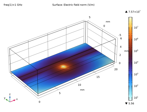
In the Settings window for 3D Plot Group, type Electric Field Norm, Differential Line in the Label text field.
|
|
1
|
|
2
|

|
1
|
|
2
|
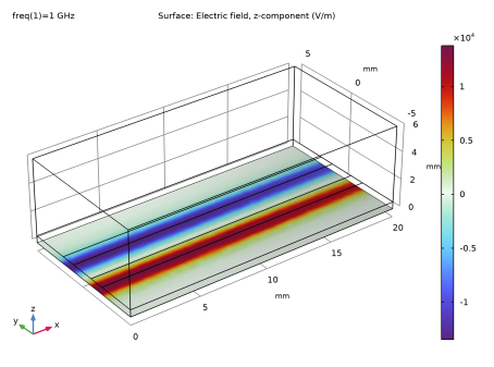
In the Settings window for 3D Plot Group, type Electric Field Ez, Differential Line in the Label text field.
|
|
3
|
Locate the Data section. From the Dataset list, choose Study 3, Differential Line/Solution 5 (sol5).
|
|
1
|
|
2
|
|
3
|
|
4
|
|
5
|
|
6
|
Click OK.
|
|
1
|
|
3
|
|
1
|
|
2
|
|
3
|
Find the Studies subsection. In the Select Study tree, select Preset Studies for Selected Physics Interfaces>TEM Boundary Mode Analysis.
|
|
4
|
|
5
|
|
1
|
In the Settings window for TEM Boundary Mode Analysis, locate the Physics and Variables Selection section.
|
|
2
|
|
3
|
In the tree, select Component 1 (comp1)>Electromagnetic Waves, Frequency Domain (emw)>Single-Ended Line Port Group.
|
|
4
|
Right-click and choose Disable.
|
|
1
|
|
2
|
|
3
|
|
4
|
In the tree, select Component 1 (comp1)>Electromagnetic Waves, Frequency Domain (emw)>Single-Ended Line Port Group.
|
|
5
|
Right-click and choose Disable.
|
|
6
|
|
7
|
In the Settings window for Study, type Study 4, Differential Line with Noise in the Label text field.
|
|
8
|
|
1
|
|
2
|
In the Settings window for Global Evaluation, type S-parameter, Differential Line with Noise in the Label text field.
|
|
1
|
|
2
|
In the Settings window for 3D Plot Group, type Electric Field Norm, Differential Line with Noise in the Label text field.
|
|
1
|
|
2
|