PDF

Electrostatic Discharge (ESD) Test of a PCB
Introduction
Electronic devices and systems are subject to electrostatic discharge (ESD) and they have to pass ESD tests according to standards. ESD tests have different levels, from component, to PCB and to system. In laboratory, ESD gun is usually used to generate discharge current which is directly or indirectly applied to electronic components. Figure 1 shows an example of a ESD test platform. The aim of the ESD test is to verify if the component or system is able to withstand ESD events. The experimental setup of an ESD test is not simple and it is only possible to test until a component or system is manufactured.
Thanks to numerical simulation, we are now able to identify ESD problems during the design stage. Moreover, numerical simulation is able to provide detailed electromagnetic field distribution which is difficult or even impossible to measure accurately. Such information is needed to understand why an ESD damage happens and how to fix it.
ESD can lead to insulating failure or logic errors to chips. The logic error can be triggered when a pin of the chip at Low state (0) experiences a voltage of amplitude larger than 1.5 V and lasting more than 1 ns, or a voltage of amplitude larger than 0.3 V and lasting more than 5 ns. This example demonstrates how an ESD event causes logic error of a microchip on a PCB board.
Figure 1: Example of an ESD test platform for a PCB.
Model Definition
ESD currents are generally very nonlinear and require a transient 3D study. The RF Module provides the Electromagnetic Waves, Transient physics interface dedicated to this purpose. This interface provides four predefined ESD currents according to different standards. These standards are the Human Body Model (HBM), Machine Model (MM), Charged Device Model (CDM), and the Extended HBM (also known as IEC 61000-4-2).
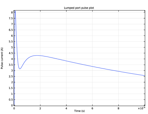
In this example, the ESD current is generated by using the Lumped Port feature with the Extended HBM, as shown in Figure 2. This current is one of the most famous test currents, since it tests against the most severe conditions. The current can easily be visualized by clicking the Plot Pulse Shape button in the Settings window.
The induced voltage at two pins of a microchip on the PCB are computed by using the Lumped Element feature. The exterior boundaries are modeled with the Scattering Boundary Condition.
Figure 2: The ESD current based on the Extended HBM.
Results and Discussion
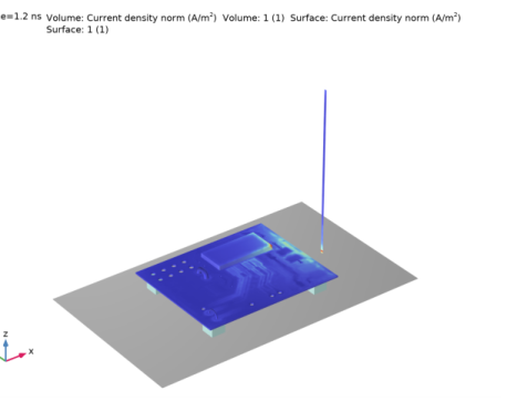
Figure 3 shows the induced surface current density by the ESD current at = 1.2 ns. Figure 4 shows the computed induced voltage at two pins (#1, #2) of the chip. As can be seen, the induced voltage at pin #2 has an amplitude higher than 1.5 V and is very likely to trigger a logic error.
Figure 3: The distribution of induced surface current density of a PCB at t = 1.2 ns due to an ESD event.
Figure 4: The induced voltage at pin #1 and pin #2 of the microchip.
Notes About the COMSOL Implementation
This example provides only a simplified modeling workflow for the virtual ESD tests. In particular, it does not comply with well-known test standards and protocols. The model setup has to be modified accordingly to perform the standard test.
Reference
1. M. Mardiguian, Electrostatic Discharge: Understand, Simulate, and Fix ESD Problems, John Wiley & Sons, 2011.
Application Library path: RF_Module/ESD_and_Lightning_Surge/esd_test_pcb
Modeling Instructions
From the File menu, choose New.
New
In the New window, click  Model Wizard.
Model Wizard
1
In the Model Wizard window, click  3D.
2
In the Select Physics tree, select Radio Frequency>Electromagnetic Waves, Transient (temw).
3
Click Add.
4
Click  Study.
5
In the Select Study tree, select General Studies>Time Dependent.
6
Geometry 1
1
In the Model Builder window, under Component 1 (comp1) click Geometry 1.
2
In the Settings window for Geometry, locate the Units section.
3
From the Length unit list, choose mm.
Import 1 (imp1)
1
In the Home toolbar, click  Import.
2
In the Settings window for Import, locate the Import section.
3
Click  Browse.
4
5
Click  Import.
Block 1 (blk1)
1
In the Geometry toolbar, click  Block.
2
In the Settings window for Block, locate the Size and Shape section.
3
In the Width text field, type 21[mm].
4
In the Depth text field, type 10[mm].
5
In the Height text field, type 1.5[mm].
6
Locate the Position section. In the x text field, type -3[mm].
7
In the y text field, type 5[mm].
8
In the z text field, type 0.508[mm].
9
Click  Build Selected.
Work Plane 1 (wp1)
1
In the Geometry toolbar, click  Work Plane.
2
In the Settings window for Work Plane, locate the Plane Definition section.
3
In the z-coordinate text field, type -5.
Work Plane 1 (wp1)>Plane Geometry
In the Model Builder window, click Plane Geometry.
Work Plane 1 (wp1)>Rectangle 1 (r1)
1
In the Work Plane toolbar, click  Rectangle.
2
In the Settings window for Rectangle, locate the Size and Shape section.
3
In the Width text field, type 100[mm].
4
In the Height text field, type 60[mm].
5
Locate the Position section. From the Base list, choose Center.
6
Click  Build Selected.
Work Plane 2 (wp2)
1
In the Model Builder window, right-click Geometry 1 and choose Work Plane.
2
In the Settings window for Work Plane, locate the Plane Definition section.
3
In the z-coordinate text field, type -5.
Work Plane 2 (wp2)>Plane Geometry
In the Model Builder window, click Plane Geometry.
Work Plane 2 (wp2)>Rectangle 1 (r1)
1
In the Work Plane toolbar, click  Rectangle.
2
In the Settings window for Rectangle, locate the Size and Shape section.
3
In the Width text field, type 5[mm].
4
In the Height text field, type 5[mm].
5
Locate the Position section. From the Base list, choose Center.
6
In the xw text field, type -20[mm].
7
In the yw text field, type -15[mm].
Work Plane 2 (wp2)>Array 1 (arr1)
1
In the Work Plane toolbar, click  Transforms and choose Array.
2
3
In the Settings window for Array, locate the Size section.
4
In the xw size text field, type 2.
5
In the yw size text field, type 2.
6
Locate the Displacement section. In the xw text field, type 40[mm].
7
In the yw text field, type 30[mm].
Extrude 1 (ext1)
1
In the Model Builder window, right-click Geometry 1 and choose Extrude.
2
In the Settings window for Extrude, locate the Distances section.
3
4
Click  Build Selected.
Work Plane 3 (wp3)
1
In the Geometry toolbar, click  Work Plane.
2
In the Settings window for Work Plane, locate the Plane Definition section.
3
From the Plane list, choose yz-plane.
4
In the x-coordinate text field, type 35[mm].
Work Plane 3 (wp3)>Plane Geometry
In the Model Builder window, click Plane Geometry.
Work Plane 3 (wp3)>Rectangle 1 (r1)
1
In the Work Plane toolbar, click  Rectangle.
2
In the Settings window for Rectangle, locate the Size and Shape section.
3
In the Width text field, type 1[mm].
4
In the Height text field, type 60[mm].
5
Locate the Position section. In the yw text field, type -5[mm].
6
Click to expand the Layers section. In the table, enter the following settings:
7
Click  Build Selected.
Work Plane 4 (wp4)
1
In the Model Builder window, right-click Geometry 1 and choose Work Plane.
2
In the Settings window for Work Plane, locate the Plane Definition section.
3
From the Plane list, choose zx-plane.
4
In the y-coordinate text field, type 4[mm].
Work Plane 4 (wp4)>Plane Geometry
In the Model Builder window, click Plane Geometry.
Work Plane 4 (wp4)>Rectangle 1 (r1)
1
In the Work Plane toolbar, click  Rectangle.
2
In the Settings window for Rectangle, locate the Size and Shape section.
3
In the Width text field, type 0.508[mm].
4
In the Height text field, type 2[mm].
5
Locate the Position section. In the yw text field, type 2[mm].
Work Plane 4 (wp4)>Rectangle 2 (r2)
1
Right-click Component 1 (comp1)>Geometry 1>Work Plane 4 (wp4)>Plane Geometry>Rectangle 1 (r1) and choose Duplicate.
2
In the Settings window for Rectangle, locate the Position section.
3
In the yw text field, type 14[mm].
4
In the Model Builder window, right-click Geometry 1 and choose Build All.
Block 2 (blk2)
1
In the Geometry toolbar, click  Block.
2
In the Settings window for Block, locate the Size and Shape section.
3
In the Width text field, type 150[mm].
4
In the Depth text field, type 150[mm].
5
In the Height text field, type 100[mm].
6
Locate the Position section. From the Base list, choose Center.
7
In the z text field, type 20[mm].
8
Click  Build All Objects.
Definitions
In the Model Builder window, expand the Component 1 (comp1)>Definitions node.
Hide for Geometry 1
1
In the Model Builder window, expand the Component 1 (comp1)>Definitions>View 1 node.
2
Right-click View 1 and choose Hide for Geometry.
3
In the Settings window for Hide for Geometry, locate the Selection section.
4
From the Geometric entity level list, choose Boundary.
5
On the object blk2, select Boundaries 2–4 only.
Printed Layer
1
In the Definitions toolbar, click  Explicit.
2
In the Settings window for Explicit, type Printed Layer in the Label text field.
3
Locate the Input Entities section. From the Geometric entity level list, choose Boundary.
4
Click  Paste Selection.
5
In the Paste Selection dialog box, type 17-19, 24, 26, 35-37, 54-57, 72-75, 86-90, 111, 112, 134, 135, 141, 142, 147-152, 154, 157, 170-172 in the Selection text field.
6
Vias
1
In the Definitions toolbar, click  Explicit.
2
In the Settings window for Explicit, type Vias in the Label text field.
3
Locate the Input Entities section. From the Geometric entity level list, choose Boundary.
4
Click  Paste Selection.
5
In the Paste Selection dialog box, type 29-32, 38-43, 52, 53, 60-63, 68-71, 78-85, 95-98, 103-110, 113-128, 136-139, 143-146, 155, 156, 158, 159, 174-179, 181-186 in the Selection text field.
6
7
In the Settings window for Explicit, locate the Input Entities section.
8
Select the Group by continuous tangent check box.
Jumpers
1
In the Definitions toolbar, click  Explicit.
2
In the Settings window for Explicit, type Jumpers in the Label text field.
3
Locate the Input Entities section. From the Geometric entity level list, choose Boundary.
4
Click  Paste Selection.
5
In the Paste Selection dialog box, type 44-51, 91-94, 99-102 in the Selection text field.
6
7
In the Settings window for Explicit, locate the Input Entities section.
8
Select the Group by continuous tangent check box.
Add Material
1
In the Home toolbar, click  Add Material to open the Add Material window.
2
Go to the Add Material window.
3
4
Click Add to Component in the window toolbar.
5
In the tree, select Built-in>FR4 (Circuit Board).
6
Right-click and choose Add to Component 1 (comp1).
Materials
FR4 (Circuit Board) (mat2)
1
In the Settings window for Material, locate the Geometric Entity Selection section.
2
Click  Paste Selection.
3
In the Paste Selection dialog box, type 2 in the Selection text field.
4
Add Material
1
Go to the Add Material window.
2
In the tree, select Built-in>Copper.
3
Click Add to Component in the window toolbar.
4
In the Home toolbar, click  Add Material to close the Add Material window.
Materials
Copper (mat3)
1
In the Settings window for Material, locate the Geometric Entity Selection section.
2
From the Geometric entity level list, choose Boundary.
3
From the Selection list, choose Printed Layer.
Spacer
1
In the Model Builder window, right-click Materials and choose Blank Material.
2
In the Settings window for Material, type Spacer in the Label text field.
3
Locate the Geometric Entity Selection section. Click  Paste Selection.
4
In the Paste Selection dialog box, type 3, 4, 6, 7 in the Selection text field.
5
6
In the Settings window for Material, locate the Material Contents section.
7
Chip
1
Right-click Materials and choose Blank Material.
2
In the Settings window for Material, type Chip in the Label text field.
3
Locate the Geometric Entity Selection section. Click  Paste Selection.
4
In the Paste Selection dialog box, type 5 in the Selection text field.
5
6
In the Settings window for Material, locate the Material Contents section.
7
Electromagnetic Waves, Transient (temw)
Perfect Electric Conductor 2
1
In the Model Builder window, under Component 1 (comp1) right-click Electromagnetic Waves, Transient (temw) and choose Perfect Electric Conductor.
2
In the Settings window for Perfect Electric Conductor, locate the Boundary Selection section.
3
From the Selection list, choose Printed Layer.
Perfect Electric Conductor 3
1
In the Physics toolbar, click  Boundaries and choose Perfect Electric Conductor.
2
In the Settings window for Perfect Electric Conductor, locate the Boundary Selection section.
3
From the Selection list, choose Vias.
Perfect Electric Conductor 4
1
In the Physics toolbar, click  Boundaries and choose Perfect Electric Conductor.
2
In the Settings window for Perfect Electric Conductor, locate the Boundary Selection section.
3
From the Selection list, choose Jumpers.
Perfect Electric Conductor 5
1
In the Physics toolbar, click  Boundaries and choose Perfect Electric Conductor.
2
In the Settings window for Perfect Electric Conductor, locate the Boundary Selection section.
3
Click  Paste Selection.
4
In the Paste Selection dialog box, type 6-9, 11, 15, 23, 163, 168, 189 in the Selection text field.
5
Perfect Electric Conductor 6
1
In the Physics toolbar, click  Boundaries and choose Perfect Electric Conductor.
2
In the Settings window for Perfect Electric Conductor, locate the Boundary Selection section.
3
Click  Paste Selection.
4
In the Paste Selection dialog box, type 191 in the Selection text field.
5
Lumped Port 1
1
In the Physics toolbar, click  Boundaries and choose Lumped Port.
2
In the Settings window for Lumped Port, locate the Boundary Selection section.
3
Click  Paste Selection.
4
In the Paste Selection dialog box, type 190 in the Selection text field.
5
6
In the Settings window for Lumped Port, locate the Lumped Port Properties section.
7
From the Terminal type list, choose Current.
8
Locate the Settings section. From the Current pulse type list, choose Electrostatic discharge.
9
From the Electrostatic discharge pulse model list, choose Extended human body model.
10
In the I01 text field, type 30[A].
11
In the I02 text field, type 5[A].
12
Click  Plot Pulse Shape for Current pulse type.
Lumped Element 1
1
In the Physics toolbar, click  Boundaries and choose Lumped Element.
2
In the Settings window for Lumped Element, locate the Boundary Selection section.
3
Click  Paste Selection.
4
In the Paste Selection dialog box, type 140 in the Selection text field.
5
Lumped Element 2
1
In the Physics toolbar, click  Boundaries and choose Lumped Element.
2
In the Settings window for Lumped Element, locate the Boundary Selection section.
3
Click  Paste Selection.
4
In the Paste Selection dialog box, type 153 in the Selection text field.
5
Scattering Boundary Condition 1
1
In the Physics toolbar, click  Boundaries and choose Scattering Boundary Condition.
2
In the Settings window for Scattering Boundary Condition, locate the Boundary Selection section.
3
Click  Paste Selection.
4
In the Paste Selection dialog box, type 1-5, 192 in the Selection text field.
5
Study 1
Step 1: Time Dependent
1
In the Model Builder window, under Study 1 click Step 1: Time Dependent.
2
In the Settings window for Time Dependent, locate the Study Settings section.
3
From the Time unit list, choose ns.
4
In the Output times text field, type range(0,0.1,10).
5
In the Model Builder window, click Study 1.
6
In the Settings window for Study, locate the Study Settings section.
7
Clear the Generate default plots check box.
Solution 1 (sol1)
1
In the Study toolbar, click  Show Default Solver.
2
In the Model Builder window, expand the Solution 1 (sol1) node, then click Time-Dependent Solver 1.
3
In the Settings window for Time-Dependent Solver, click to expand the Time Stepping section.
4
From the Steps taken by solver list, choose Manual.
5
In the Time step text field, type 0.1[ns].
6
Click  Compute.
Results
Current Density
1
In the Home toolbar, click  Add Plot Group and choose 3D Plot Group.
2
In the Settings window for 3D Plot Group, type Current Density in the Label text field.
3
Locate the Plot Settings section. Clear the Plot dataset edges check box.
Volume 1
1
Right-click Current Density and choose Volume.
2
In the Settings window for Volume, locate the Expression section.
3
In the Expression text field, type temw.normJ.
Selection 1
1
Right-click Volume 1 and choose Selection.
2
In the Settings window for Selection, locate the Selection section.
3
Click  Paste Selection.
4
In the Paste Selection dialog box, type 2,5 in the Selection text field.
5
Volume 2
1
In the Model Builder window, right-click Current Density and choose Volume.
2
In the Settings window for Volume, locate the Expression section.
3
In the Expression text field, type 1.
4
Locate the Coloring and Style section. From the Coloring list, choose Uniform.
5
From the Color list, choose Custom.
6
7
Click Define custom colors.
8
9
Click Add to custom colors.
10
Click Show color palette only or OK on the cross-platform desktop.
Selection 1
1
Right-click Volume 2 and choose Selection.
2
In the Settings window for Selection, locate the Selection section.
3
Click  Paste Selection.
4
In the Paste Selection dialog box, type 3, 4, 6, 7 in the Selection text field.
5
Surface 1
1
In the Model Builder window, right-click Current Density and choose Surface.
2
In the Settings window for Surface, locate the Expression section.
3
In the Expression text field, type temw.normJ.
Selection 1
1
Right-click Surface 1 and choose Selection.
2
In the Settings window for Selection, locate the Selection section.
3
Click  Paste Selection.
4
In the Paste Selection dialog box, type 190, 191 in the Selection text field.
5
Surface 2
1
In the Model Builder window, right-click Current Density and choose Surface.
2
In the Settings window for Surface, locate the Expression section.
3
In the Expression text field, type 1.
4
Locate the Coloring and Style section. From the Coloring list, choose Uniform.
5
From the Color list, choose Gray.
Selection 1
1
Right-click Surface 2 and choose Selection.
2
In the Settings window for Selection, locate the Selection section.
3
Click  Paste Selection.
4
In the Paste Selection dialog box, type 6 in the Selection text field.
5
Current Density
1
In the Model Builder window, under Results click Current Density.
2
In the Current Density toolbar, click  Plot.
3
Click the  Show Legends button in the Graphics toolbar.
4
Click the  Show Grid button in the Graphics toolbar.
5
Click the  Go to Default View button in the Graphics toolbar.
6
In the Settings window for 3D Plot Group, locate the Data section.
7
From the Time (ns) list, choose 1.2.
8
In the Current Density toolbar, click  Plot.
Induced Voltage
1
In the Home toolbar, click  Add Plot Group and choose 1D Plot Group.
2
In the Settings window for 1D Plot Group, type Induced Voltage in the Label text field.
Global 1
1
Right-click Induced Voltage and choose Global.
2
In the Settings window for Global, click Replace Expression in the upper-right corner of the y-Axis Data section. From the menu, choose Component 1 (comp1)>Electromagnetic Waves, Transient>Lumped elements>temw.Velement_1 - Lumped element voltage - V.
3
Locate the y-Axis Data section. In the table, enter the following settings:
4
Click to expand the Legends section. From the Legends list, choose Manual.
5
6
In the Induced Voltage toolbar, click  Plot.