You are viewing the documentation for an older COMSOL version. The latest version is available here.
PDF

Coplanar Waveguide Bandpass Filter
Introduction
Coplanar waveguide (CPW) bandpass filters can be realized using interdigital capacitors (IDCs) and short-circuited stub inductors (SSIs). Such a filter can readily be implemented on a GaAs wafer. The presented model is compact in relation to its resonant frequency and provides a relatively high Q factor compared to capacitively coupled microstrip line model designs.
Figure 1: A coplanar waveguide bandpass filter on a 200 μm GaAs wafer composed of an interdigital capacitor and short-circuited stub inductors.
Model Definition
The structure shown in Figure 1 can be realized by etching a pattern in a thin gold layer on a high dielectric (εr = 12.9) GaAs substrate. In this model, the gold layer is treated as an infinitely thin layer of perfectly conducting material. Two lumped ports represent a coplanar waveguide coupling into, and out of, the device. The lumped port applies a voltage difference between the center conductor and the ground planes. This voltage difference is applied through the multielement uniform type of a lumped port that equally divides the signal between two ground planes. The line width and coupling gap on the comb in the interdigital capacitor is 100 microns, which is wide enough to account for etching tolerances. Series and parasitic SSIs are added to generate a bandpass frequency response.
The model space consists of the GaAs wafer, with the pattern on the surface, and an air box surrounding the entire structure. The air box, in turn, is bounded by a perfect electric conductor boundary representing a die packaging placed far enough from the CPW so as not to introduce any unwanted coupling.
Results and Discussion
The structure is simulated over a range of frequencies from 7.1 GHz to 8.1 GHz. The simulation results show bandpass filter characteristics around 7.65 GHz as presented in Figure 2.
Because the filter is enclosed by the PEC package, it is effectively a grounded coplanar waveguide circuit and there is a parasitic reactance between the circuit and the bottom ground plane. This reactance loading produces wider frequency responses than those generated from the circuit itself. The model without the package as well as the bottom ground plane provides sharper frequency responses.
It is generally recommended to add air bridges around SSIs when structures of this type are used for very high frequencies in order to suppress any potential radiation over the slots.
Figure 2: The frequency response of the coplanar waveguide filter shows bandpass characteristics around 7.65GHz.
Application Library path: RF_Module/Filters/cpw_bandpass_filter
Modeling Instructions
From the File menu, choose New.
New
In the New window, click  Model Wizard.
Model Wizard
1
In the Model Wizard window, click  3D.
2
In the Select Physics tree, select Radio Frequency>Electromagnetic Waves, Frequency Domain (emw).
3
Click Add.
4
Click  Study.
5
In the Select Study tree, select Preset Studies for Selected Physics Interfaces>Frequency Domain, Modal.
6
Study 1
Step 1: Eigenfrequency
1
In the Model Builder window, under Study 1 click Step 1: Eigenfrequency.
2
In the Settings window for Eigenfrequency, locate the Study Settings section.
3
In the Search for eigenfrequencies around text field, type 7.1[GHz].
Step 2: Frequency Domain, Modal
1
In the Model Builder window, click Step 2: Frequency Domain, Modal.
2
In the Settings window for Frequency Domain, Modal, locate the Study Settings section.
3
Click  Range.
4
In the Range dialog box, type 7.1[GHz] in the Start text field.
5
In the Step text field, type 2[MHz].
6
In the Stop text field, type 8.1[GHz].
7
Click Replace.
Geometry 1
1
In the Model Builder window, under Component 1 (comp1) click Geometry 1.
2
In the Settings window for Geometry, locate the Units section.
3
From the Length unit list, choose µm.
Import 1 (imp1)
1
In the Home toolbar, click  Import.
2
In the Settings window for Import, locate the Import section.
3
Click  Browse.
4
5
Click  Import.
6
Click the  Wireframe Rendering button in the Graphics toolbar.
Add Material
1
In the Home toolbar, click  Add Material to open the Add Material window.
2
Go to the Add Material window.
3
4
Click Add to Component in the window toolbar.
5
In the Home toolbar, click  Add Material to close the Add Material window.
Materials
GaAs
1
In the Model Builder window, under Component 1 (comp1) right-click Materials and choose Blank Material.
2
In the Settings window for Material, type GaAs in the Label text field.
3
4
Locate the Material Contents section. In the table, enter the following settings:
Definitions
In the Model Builder window, expand the Component 1 (comp1)>Definitions node.
View 1
Before setting up the physics, hide the air domain to get a better view and easier access to the CPW circuit geometry.
Hide for Physics 1
1
In the Model Builder window, expand the Component 1 (comp1)>Definitions>View 1 node.
2
Right-click View 1 and choose Hide for Physics.
3
Electromagnetic Waves, Frequency Domain (emw)
Perfect Electric Conductor 2
1
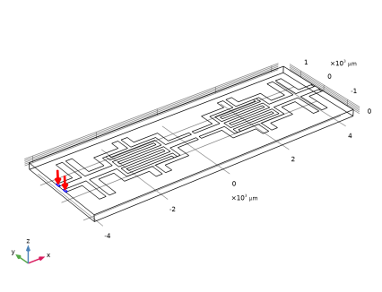
In the Model Builder window, under Component 1 (comp1) right-click Electromagnetic Waves, Frequency Domain (emw) and choose the boundary condition Perfect Electric Conductor.
2
Excite and terminate each end of the CPW line using multielement uniform lumped ports.
Lumped Port 1
1
In the Physics toolbar, click  Boundaries and choose Lumped Port.
2
3
In the Settings window for Lumped Port, locate the Lumped Port Properties section.
4
From the Type of lumped port list, choose Multielement uniform.
For the first port, wave excitation is on by default.
5
Locate the Boundary Selection section. Click  Create Selection.
6
In the Create Selection dialog box, Create a set of selections for use in the study settings.
7
type Lumped Port 1 in the Selection name text field.
8
Uniform Element 1
1
In the Model Builder window, expand the Lumped Port 1 node, then click Uniform Element 1.
2
In the Settings window for Uniform Element, locate the Boundary Selection section.
3
Click  Clear Selection.
4
5
Locate the Uniform Element Properties section. Specify the ah vector as
Uniform Element 2
1
In the Model Builder window, click Uniform Element 2.
2
3
In the Settings window for Uniform Element, locate the Uniform Element Properties section.
4
Specify the ah vector as
Lumped Port 2
1
In the Physics toolbar, click  Boundaries and choose Lumped Port.
2
3
In the Settings window for Lumped Port, locate the Lumped Port Properties section.
4
From the Type of lumped port list, choose Multielement uniform.
5
Locate the Boundary Selection section. Click  Create Selection.
6
In the Create Selection dialog box, type Lumped Port 2 in the Selection name text field.
7
Uniform Element 1
1
In the Model Builder window, expand the Lumped Port 2 node, then click Uniform Element 1.
2
In the Settings window for Uniform Element, locate the Boundary Selection section.
3
Click  Clear Selection.
4
5
Locate the Uniform Element Properties section. Specify the ah vector as
Uniform Element 2
1
In the Model Builder window, click Uniform Element 2.
2
3
In the Settings window for Uniform Element, locate the Uniform Element Properties section.
4
Specify the ah vector as
Mesh 1
1
In the Model Builder window, under Component 1 (comp1) right-click Mesh 1 and choose Build All.
The default frequency and material-dependent physics-controlled mesh is not fine enough to accurately evaluate the reactance of the comb structures in the IDCs. Refine the mesh settings manually.
2
In the Settings window for Mesh, locate the Sequence Type section.
3
From the list, choose User-controlled mesh.
Size 1
1
In the Model Builder window, right-click Free Tetrahedral 1 and choose Size.
2
In the Settings window for Size, locate the Geometric Entity Selection section.
3
From the Geometric entity level list, choose Boundary.
4
Click  Paste Selection.
5
In the Paste Selection dialog box, type 13-26 in the Selection text field.
6
7
In the Settings window for Size, locate the Element Size section.
8
Click the Custom button.
9
Locate the Element Size Parameters section.
10
Select the Maximum element size check box. In the associated text field, type 80.
11
Click  Build All.
12
Click the  Zoom Extents button in the Graphics toolbar.
Study 1
Step 2: Frequency Domain, Modal
1
In the Model Builder window, under Study 1 click Step 2: Frequency Domain, Modal.
2
In the Settings window for Frequency Domain, Modal, click to expand the Values of Dependent Variables section.
3
Find the Store fields in output subsection. From the Settings list, choose For selections.
4
Under Selections, click  Add.
5
In the Add dialog box, in the Selections list, choose Lumped Port 1 and Lumped Port 2.
6
7
In the Home toolbar, click  Compute.
Results
Electric Field (emw)
Since the results of the Frequency Domain Modal analysis are stored only on the lumped port boundaries, this default E-field norm plot does not provide useful information. Switch the dataset to the solution of the Eigenfrequency analysis.
1
In the Settings window for 3D Plot Group, locate the Data section.
2
From the Dataset list, choose Study 1/Solution Store 1 (sol2).
Multislice
1
In the Model Builder window, expand the Electric Field (emw) node, then click Multislice.
2
In the Settings window for Multislice, locate the Multiplane Data section.
3
Find the X-planes subsection. In the Planes text field, type 0.
4
Find the Y-planes subsection. In the Planes text field, type 0.
5
Find the Z-planes subsection. From the Entry method list, choose Coordinates.
6
In the Coordinates text field, type 0.
7
In the Electric Field (emw) toolbar, click  Plot.
S-parameter (emw)
1
In the Model Builder window, under Results click S-parameter (emw).
2
In the Settings window for 1D Plot Group, locate the Legend section.
3
From the Position list, choose Lower right.
The S-parameter plot is shown in Figure 2.
Smith Plot (emw)