PDF

Antenna Decoupling Using an Electromagnetic Band Gap Metamaterial
Introduction
An electromagnetic band gap (EBG) structure can be used to increase the isolation between antennas that are close to each other. This decoupling effect is not only a function of frequency but also of polarization and coupling-plane configuration. In this example, an EBG structure is placed between two antennas. The solution shows a marked decrease in coupling between the two antennas.
Figure 1: Two 90° bent monopole antennas over a thick substrate separated by electromagnetic band gap structures.
Model Definition
An electromagnetic band gap structure can strongly inhibit the propagation of an electromagnetic wave. Although there are many different structures that can exhibit a band gap, such structures are almost always initially designed at the unit cell level. That is, a single element of the EBG structure is assumed to be patterned infinitely through space, and a separate analysis is performed to find the band gaps.
Once the EBG structure has been engineered to achieve the desired band gap, for an infinite structure, it can be used in a finite-sized space. However, the properties of the structure change slightly because the assumption of infinite periodicity used to compute the band gaps does not hold any longer. Therefore, it is necessary to compute the performance of an EBG structure in real space.
This example starts with an EBG structure composed of metallic mushrooms that has already been engineered to have a band gap centered at 1.85 GHz. One row of these mushroom structures are placed between two antennas, as shown in Figure 1. A typical use of such an EBG structure is to provide isolation between the elements of an array antenna. This example uses only two antenna elements to demonstrate the concept.
The antenna elements are metal strips, fed by a coaxial cable, sitting above a dielectric substrate on top of the ground plane. Although these are not typical antenna elements, they are used because they highlight the effectiveness of the isolation provided by the mushroom structures. In this analysis only one antenna element is excited, while the other acts as a receiver to determine the coupling.
The antenna array structure is modeled inside an air sphere truncated by a Perfectly Matched Layer, which allows the antenna to radiate freely in all directions. The antenna characteristics are not of primary interest here, however.
The model can be run both with and without the EBG mushroom structures, of which only the former case is considered here. The model is simulated over a range of frequencies around the band gap to observe the change in S21.
Results and Discussion
Figure 2 plots S21 for the case of the antenna array with and without the EBG structure, showing a marked improvement when adding the EBG. Because the model only uses a single row of five mushroom elements, the maximum isolation is not exactly at the frequency predicted by the band-gap analysis.
Figure 2: The frequency response of the coupling between two antennas with/without EBG structures shows the decoupling effect around 2.2 GHz.
Figure 3: Electric field with EBG (left) and without EBG structures (right).
Two coaxial lumped ports are applied and S21 is observed with/without the five EBG structures. As shown in Figure 2, a part of the frequency band has stronger coupling with the EBG structures and the decoupling bandwidth is not wide. The center frequency of the decoupling band is also a function of the configuration of the coupling plane of the two antennas, and adding the EBG structures does not always guarantee better isolation between antennas.
Reference
1. M. Tan. T.A. Rahman, S.K.A. Rahim, M.T. Ali, and M.F. Jamlos, “Antenna array enhancement using mushroom-like electromagnetic band gap (EBG)”, Antennas and Propagation (EuCAP), Proc. 4th European Conf., 2010.
Application Library path: RF_Module/EMI_EMC_Applications/antenna_ebg
Modeling Instructions
From the File menu, choose New.
New
In the New window, click  Model Wizard.
Model Wizard
1
In the Model Wizard window, click  3D.
2
In the Select Physics tree, select Radio Frequency>Electromagnetic Waves, Frequency Domain (emw).
3
Click Add.
4
Click  Study.
5
In the Select Study tree, select General Studies>Frequency Domain.
6
Study 1
Step 1: Frequency Domain
1
In the Model Builder window, under Study 1 click Step 1: Frequency Domain.
2
In the Settings window for Frequency Domain, locate the Study Settings section.
3
In the Frequencies text field, type range(2.1[GHz],10[MHz],2.35[GHz]).
You can alternatively set the simulation frequency range by clicking the Range button next to the Frequencies text field.
Geometry 1
1
In the Model Builder window, under Component 1 (comp1) click Geometry 1.
2
In the Settings window for Geometry, locate the Units section.
3
From the Length unit list, choose mm.
Create a substrate.
Substrate
1
In the Geometry toolbar, click  Block.
2
In the Settings window for Block, type Substrate in the Label text field.
3
Locate the Size and Shape section. In the Width text field, type 60.
4
In the Depth text field, type 80.
5
In the Height text field, type 12.
6
Locate the Position section. In the x text field, type -30.
7
In the y text field, type -40.
8
Click  Build Selected.
9
Click the  Wireframe Rendering button in the Graphics toolbar.
Create a mushroom.
Work Plane 1 (wp1)
1
In the Geometry toolbar, click  Work Plane.
2
In the Settings window for Work Plane, locate the Plane Definition section.
3
In the z-coordinate text field, type 12.
4
Click  Show Work Plane.
Work Plane 1 (wp1)>Square 1 (sq1)
1
In the Work Plane toolbar, click  Square.
2
In the Settings window for Square, locate the Size section.
3
In the Side length text field, type 8.
4
Locate the Position section. From the Base list, choose Center.
5
In the xw text field, type -24.
6
Click  Build Selected.
Mushroom
1
In the Model Builder window, under Component 1 (comp1)>Geometry 1 click Work Plane 1 (wp1).
2
In the Settings window for Work Plane, type Mushroom in the Label text field.
Mushroom Stem
1
In the Geometry toolbar, click  Block.
2
In the Settings window for Block, type Mushroom Stem in the Label text field.
3
Locate the Size and Shape section. In the Height text field, type 12.
4
Locate the Position section. In the x text field, type -24.5.
5
In the y text field, type -0.5.
6
Click  Build Selected.
Create an array of mushrooms.
EBG Structure
1
In the Geometry toolbar, click  Transforms and choose Array.
2
In the Settings window for Array, type EBG Structure in the Label text field.
3
Select the objects blk2 and wp1 only.
4
Locate the Size section. In the x size text field, type 5.
5
Locate the Displacement section. In the x text field, type 12.
6
Click  Build All Objects.
Create a coax inner conductor.
Cylinder 1 (cyl1)
1
In the Geometry toolbar, click  Cylinder.
2
In the Settings window for Cylinder, locate the Size and Shape section.
3
In the Radius text field, type 0.5.
4
In the Height text field, type 14.
5
Locate the Position section. In the x text field, type -10.
6
In the y text field, type -20.
7
Click  Build Selected.
Create a coax outer conductor.
Cylinder 2 (cyl2)
1
In the Geometry toolbar, click  Cylinder.
2
In the Settings window for Cylinder, locate the Size and Shape section.
3
In the Radius text field, type 2.35.
4
In the Height text field, type 12.
5
Locate the Position section. In the x text field, type -10.
6
In the y text field, type -20.
7
Click  Build Selected.
Create an antenna radiator.
Block 3 (blk3)
1
In the Geometry toolbar, click  Block.
2
In the Settings window for Block, locate the Size and Shape section.
3
In the Width text field, type 25.
4
In the Depth text field, type 2.
5
Locate the Position section. In the x text field, type -10.
6
In the y text field, type -21.
7
In the z text field, type 13.
8
Click  Build Selected.
Create a pair of 90-degree bent monopole antennas.
Copy 1 (copy1)
1
In the Geometry toolbar, click  Transforms and choose Copy.
2
Select the objects blk3, cyl1, and cyl2 only.
3
In the Settings window for Copy, locate the Displacement section.
4
In the y text field, type 40.
5
Click  Build Selected.
Create a sphere for PML layers and an air domain.
Sphere 1 (sph1)
1
In the Geometry toolbar, click  Sphere.
2
In the Settings window for Sphere, locate the Size section.
3
In the Radius text field, type 100.
4
Click to expand the Layers section. In the table, enter the following settings:
5
Click  Build All Objects.
6
Click the  Zoom Extents button in the Graphics toolbar.
Definitions
Internal PEC Boundaries
1
In the Definitions toolbar, click  Explicit.
2
In the Settings window for Explicit, type Internal PEC Boundaries in the Label text field.
3
Locate the Input Entities section. From the Geometric entity level list, choose Boundary.
4
Perfectly Matched Layer 1 (pml1)
1
In the Definitions toolbar, click  Perfectly Matched Layer.
2
3
In the Settings window for Perfectly Matched Layer, locate the Geometry section.
4
From the Type list, choose Spherical.
Hide some domains to get a better view of the interior parts.
Definitions
Hide for Physics 1
1
In the Model Builder window, right-click View 1 and choose Hide for Physics.
2
Electromagnetic Waves, Frequency Domain (emw)
Perfect Electric Conductor 2
1
In the Model Builder window, under Component 1 (comp1) right-click Electromagnetic Waves, Frequency Domain (emw) and choose the boundary condition Perfect Electric Conductor.
2
In the Settings window for Perfect Electric Conductor, locate the Boundary Selection section.
3
From the Selection list, choose Internal PEC Boundaries.
Perfect Electric Conductor 3
1
In the Physics toolbar, click  Domains and choose Perfect Electric Conductor.
2
Lumped Port 1
1
In the Physics toolbar, click  Boundaries and choose Lumped Port.
2
Click the  Zoom In button in the Graphics toolbar, two or three times.
3
4
In the Model Builder window, click Lumped Port 1.
5
In the Settings window for Lumped Port, locate the Lumped Port Properties section.
6
From the Type of lumped port list, choose Coaxial.
For the first port, wave excitation is on by default.
Lumped Port 2
1
In the Physics toolbar, click  Boundaries and choose Lumped Port.
2
3
In the Settings window for Lumped Port, locate the Lumped Port Properties section.
4
From the Type of lumped port list, choose Coaxial.
Add Material
1
In the Home toolbar, click  Add Material to open the Add Material window.
2
Go to the Add Material window.
3
4
Click Add to Component in the window toolbar.
5
In the Home toolbar, click  Add Material to close the Add Material window.
Materials
Air (mat1)
Override this material for the substrate and coaxial cable domains.
Substrate
1
In the Model Builder window, right-click Materials and choose Blank Material.
2
In the Settings window for Material, type Substrate in the Label text field.
3
4
Locate the Material Contents section. In the table, enter the following settings:
PTFE
1
Right-click Materials and choose Blank Material.
2
In the Settings window for Material, type PTFE in the Label text field.
3
4
Locate the Material Contents section. In the table, enter the following settings:
Mesh 1
1
In the Model Builder window, under Component 1 (comp1) right-click Mesh 1 and choose Build All.
2
Click the  Zoom Extents button in the Graphics toolbar.
3
Click the  Zoom In button in the Graphics toolbar.
4
Click the  Reset Hiding button in the Graphics toolbar, to reset the visibility state of the hidden domains in preparation of the results processing.
Study 1
In the Home toolbar, click  Compute.
Results
Electric Field (emw)
1
In the Settings window for 3D Plot Group, locate the Data section.
2
From the Parameter value (freq (GHz)) list, choose 2.2.
3
Click to expand the Title section. From the Title type list, choose None.
Multislice
1
In the Model Builder window, expand the Electric Field (emw) node, then click Multislice.
2
In the Settings window for Multislice, locate the Multiplane Data section.
3
Find the X-planes subsection. In the Planes text field, type 0.
4
Find the Y-planes subsection. In the Planes text field, type 0.
5
Find the Z-planes subsection. From the Entry method list, choose Coordinates.
6
In the Coordinates text field, type 12.5.
7
Locate the Expression section. In the Expression text field, type 20*log10(emw.normE).
8
Locate the Coloring and Style section. Clear the Color legend check box.
9
In the Electric Field (emw) toolbar, click  Plot.
10
Click the  Zoom Extents button in the Graphics toolbar.
11
Click the  Zoom In button in the Graphics toolbar.
The following instructions reproduce the frequency-response plot shown in Figure 2:
Global 1
1
In the Model Builder window, expand the Results>S-parameter (emw) node, then click Global 1.
2
In the Settings window for Global, click to expand the Legends section.
3
From the Legends list, choose Manual.
4
S-parameter (emw)
1
In the Model Builder window, click S-parameter (emw).
2
In the Settings window for 1D Plot Group, click to expand the Title section.
3
From the Title type list, choose None.
4
In the S-parameter (emw) toolbar, click  Plot.
To re-solve the model without EBG mushroom structures, do as follows:
Under Model 1>Geometry 1 select Mushroom, Mushroom Stem, and EBG Structure, choose Disable.
Right-click Study 1 and choose Compute.
The computation takes about 10 minutes. Here, the table with computed S21 parameter values is imported for convenience.
Table 1
1
In the Results toolbar, click  Table.
2
In the Settings window for Table, locate the Data section.
3
Click Import.
4
Table Graph 1
1
Right-click S-parameter (emw) and choose Table Graph.
2
In the Settings window for Table Graph, click to expand the Legends section.
3
Select the Show legends check box.
4
From the Legends list, choose Manual.
5
6
In the S-parameter (emw) toolbar, click  Plot.
Smith Plot (emw)
Analyze the same model with a much finer frequency resolution using Adaptive Frequency Sweep based on asymptotic waveform evaluation (AWE). When a device presents a slowly varying frequency response, the AWE method provides a faster solution time when running the simulation on many frequency points. The following example with the Adaptive Frequency Sweep can be computed five times faster than regular Frequency Domain sweeps with a same finer frequency resolution.
Electromagnetic Waves, Frequency Domain (emw)
Lumped Port 1
1
In the Model Builder window, under Component 1 (comp1)>Electromagnetic Waves, Frequency Domain (emw) click Lumped Port 1.
2
In the Settings window for Lumped Port, locate the Boundary Selection section.
3
Click  Create Selection.
4
In the Create Selection dialog box, type Lumped port 1 in the Selection name text field.
5
Lumped Port 2
1
In the Model Builder window, click Lumped Port 2.
2
In the Settings window for Lumped Port, locate the Boundary Selection section.
3
Click  Create Selection.
4
In the Create Selection dialog box, type Lumped port 2 in the Selection name text field.
5
Add Study
1
In the Home toolbar, click  Add Study to open the Add Study window.
2
Go to the Add Study window.
3
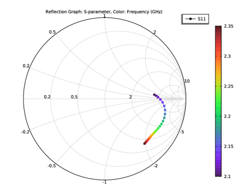
Find the Studies subsection. In the Select Study tree, select Preset Studies for Selected Physics Interfaces>Adaptive Frequency Sweep.
4
Click Add Study in the window toolbar.
5
In the Home toolbar, click  Add Study to close the Add Study window.
Study 2
Step 1: Adaptive Frequency Sweep
1
In the Settings window for Adaptive Frequency Sweep, locate the Study Settings section.
2
In the Frequencies text field, type range(2.1[GHz],2[MHz],2.35[GHz]).
Use a five times finer frequency resolution.
3
From the AWE expression type list, choose User controlled.
4
A slowly varying scalar value curve works well for AWE expression. Use abs(comp1.emw.S11) for this model.
Because such a fine frequency step generates a memory-intensive solution, the model file size will increase tremendously when it is saved. When only the frequency response of port related variables are of interest, it is not necessary to store all of the field solutions. By selecting the Store fields in output check box in the Values of Dependent Variables section, we can control the part of the model on which the computed solution is saved. We only add the selection containing these boundaries where the port variables are calculated. The lumped port size is typically very small compared to the entire modeling domain, and the saved file size with the fine frequency step is more or less that of the regular discrete frequency sweep model when only the solutions on the port boundaries are stored.
5
Locate the Values of Dependent Variables section. Find the Store fields in output subsection. From the Settings list, choose For selections.
6
Under Selections, click  Add.
7
In the Add dialog box, in the Selections list, choose Lumped port 1 and Lumped port 2.
8
It is necessary to include the lumped port boundaries to calculate S-parameters. By choosing only the lumped port boundaries for Store fields in output settings, it is possible to reduce the size of a model file a lot.
9
In the Home toolbar, click  Compute.
Results
Multislice
1
In the Model Builder window, expand the Electric Field (emw) 1 node.
2
Right-click Results>Electric Field (emw) 1>Multislice and choose Delete.
Surface 1
In the Model Builder window, right-click Electric Field (emw) 1 and choose Surface.
Selection 1
1
In the Model Builder window, right-click Surface 1 and choose Selection.
2
3
In the Electric Field (emw) 1 toolbar, click  Plot.
S-parameter (emw) 1
1
In the Model Builder window, under Results click S-parameter (emw) 1.
2
In the Settings window for 1D Plot Group, locate the Legend section.
3
From the Position list, choose Middle right.
Global 1
1
In the Model Builder window, expand the S-parameter (emw) 1 node, then click Global 1.
2
In the Settings window for Global, locate the y-Axis Data section.
3
Global 2
1
Right-click Results>S-parameter (emw) 1>Global 1 and choose Duplicate.
2
In the Settings window for Global, locate the y-Axis Data section.
3
4
Locate the Data section. From the Dataset list, choose Study 1/Solution 1 (sol1).
5
Click to expand the Coloring and Style section. Find the Line style subsection. From the Line list, choose Dotted.
6
Find the Line markers subsection. From the Marker list, choose Cycle.
7
In the S-parameter (emw) 1 toolbar, click  Plot.
Smith Plot (emw) 1