PDF

Thin-Film BAW Composite Resonator
Introduction
Bulk acoustic wave (BAW) resonators can be used as narrow band filters in radio-frequency applications. Their chief advantage compared with traditional ceramic electromagnetic resonators is that they can be made smaller in size because they can be designed to have an acoustic wavelength smaller than the electromagnetic wavelength.
In addition to the desired bulk acoustic mode, the resonator structure may have many spurious modes with very narrow spacing. The design goal is usually to maximize the quality of the main component and to reduce the effect of spurious modes.
This tutorial shows how you can model thin-film BAW resonators in 2D using eigenfrequency and frequency-response analyses. The geometry used here is the same as that in Ref. 1 and Ref. 2.
Figure 1: Arbitrarily scaled geometry of a thin film BAW resonator.
Model Definition
Figure 1 shows the geometry of the resonator from Ref. 1. The lowest layer of the resonator is silicon. On top of that, there is an aluminum layer that operates as the ground electrode. Above the aluminum layer is the active piezoelectric layer made of zinc oxide (ZnO). The topmost layer of the resonator is an aluminum electrode. The material properties used in this model are obtained from the MEMS Module material library.
A large part of the silicon layer is etched away from the lower end of the central region of the resonator structure. This effectively reduces the thickness of the active central region thereby making the device a thin-film composite BAW resonator.
The thickness of the silicon layer at the central region is 7 μm. Both aluminum layers are 0.2 μm thick, and the piezoelectric layer is 9.5 μm thick. The width of the rectangular top electrode is 500 μm. The thin silicon area is roughly 1.7 mm wide.
Figure 2: The 2D geometry (not drawn to scale) used in the tutorial.
This example is modeled in 2D, using the plane strain assumption where the out-of-plane thickness is specified to be 1.7 mm. The modeled geometry (Figure 2) is a symmetric 1-mm section in the center of the resonator. The Perfectly Matched Layer (PML) domains used on the two sides effectively increase the length of the resonator and simulates the effect of propagation and absorption of elastic waves in the adjoining regions which are not resolved in the true geometric scale.
The absorption of elastic waves in the PML domains contribute to the damping of the structure. This is also known as anchor loss. Additionally, the model also incorporates mechanical and electrical losses in the piezoelectric zinc oxide layer by means of loss factors. A structural loss factor represents the hysteresis in a stress-strain curve and a dielectric loss factor represents the polarization loss, which manifests itself as the hysteresis in the polarization versus electric field curve of the material. The structural and dielectric loss factors appear as the imaginary components of the mechanical stiffness and relative permittivity, respectively.
Ref. 3 gives the material quality Qm and the dielectric loss tangent tan δ for many materials. The magnitude of Qm is roughly 1001000, and the magnitude of tan δ is roughly 0.0010.01. Based on that data, the following values are used:
In this model, COMSOL Multiphysics solves for both structural and electrical equations in the piezoelectric layer but only solves for the structural equation in the other layers. The electrical equations are not solved in the metallic aluminum layers because the electrical conductivity of aluminum is several orders of magnitude higher than that of zinc oxide and hence the aluminum layers almost act as equipotential regions allowing extremely small conduction current through them. Therefore the electrical characteristics of aluminum do not have any significant effect on the response of the resonator. The dominant electromechanical coupling is exhibited by the piezoelectric layer only.
This tutorial shows two different analyses. In the first step, you compute and investigate the eigenmodes of the structure, with its lateral ends fixed. In the second step, you analyze the frequency response of the resonator within the desired bandwidth of 215 MHz to 235 MHz.
Results and Discussion
Figure 3 shows the lowest BAW mode of the structure which occurs at 221.4 MHz. This plot was generated from the results of the eigenfrequency analysis. This is the fundamental longitudinal thickness mode. The plot shows scaled deformation only to be used for visualization of the mode shape. Note that COMSOL Multiphysics computes complex-valued eigenfrequencies where the imaginary part gives a measure of the damping due to structural loss, polarization loss and anchor loss.
Figure 3: The lowest bulk acoustic mode of the resonator identified from the solutions of the eigenfrequency analysis.
Figure 4: The lowest bulk acoustic mode of the resonator identified from the solutions of the frequency domain analysis.
Figure 4 shows the deformation of the resonator obtained from the frequency response analysis when the zinc oxide layer is excited with 1 volt (zero-to-peak voltage) at 221.5 MHz. The maximum deflection is about 3 nm.
Figure 5: Electric potential distribution in the zinc oxide layer at 235 MHz excitation.
Figure 5 shows the voltage distribution in the piezoelectric layer when excited at 235 MHz.
The Terminal boundary condition in COMSOL Multiphysics, which is used to specify the voltage on the piezoelectric material, also automatically computes the admittance. The admittance is the ratio of the total current flowing through the piezoelectric material to the voltage across it. It is a complex-valued quantity for a lossy material. Typically the imaginary part reflects the displacement current and the real part reflects the conduction current as well as other losses in the structure. Figure 6 shows the absolute value of admittance as a function of frequency. Within the investigated range of 215 MHz to 235 MHz, the admittance is very similar to that shown in Ref. 2. Note that the highest peak in admittance occurs at the lowest BAW mode of 221 MHz.
Figure 6: Absolute value of the admittance vs. frequency.
Figure 7: Quality factor vs. frequency.
Figure 7 shows the quality factor of the device as a function of frequency. The quality factor or Q factor indicates the number of cycles (at the given frequency) in which the total energy of the system decreases by a factor of e2π. This is also automatically computed by COMSOL Multiphysics. Figure 7 shows that the maximum value of Q ~ 1300 is obtained at around 221 MHz. This value obtained from the frequency-response analysis agrees well with the Q factor computed by the eigenfrequency analysis. The results from the eigenfrequency analysis shows the Q factor at 221.4 MHz to be 1326.
The eigenfrequency analysis also automatically computes the decay factor for each eigenfrequency. The inverse of the decay factor is the time required for the amplitude of a damped signal to reduce to e1 of its initial amplitude. The decay factor at 221.4 MHz was computed to be 5.25 · 105 s1.
References
1. R.F. Milsom, J.E., Curran, S.L. Murray, S. Terry-Wood, and M. Redwood, “Effect of Mesa-Shaping on Spurious Modes in ZnO/Si Bulk-Wave Composite Resonators,” Proc. IEEE Ultrason. Symp., pp. 498–503, 1983.
2. T. Makkonen, A. Holappa, J. Ellä, and M.M. Salomaa, “Finite element simulations of thin-film composite BAW resonators,” IEEE Transactions on Ultrasonics, Ferroelectrics, and Frequency Control, vol. 48, no. 5, 2001.
3. Morgan Advanced Materials, http://www.morganelectroceramics.com
Application Library path: MEMS_Module/Piezoelectric_Devices/thin_film_baw_resonator
Modeling Instructions
From the File menu, choose New.
New
In the New window, click  Model Wizard.
Model Wizard
1
In the Model Wizard window, click  2D.
2
In the Select Physics tree, select Structural Mechanics>Electromagnetics-Structure Interaction>Piezoelectricity>Piezoelectricity, Solid.
3
Click Add.
4
Click  Study.
5
In the Select Study tree, select Preset Studies for Selected Multiphysics>Eigenfrequency.
6
Geometry 1
1
In the Geometry toolbar, click  Sketch.
2
In the Model Builder window, click Geometry 1.
3
In the Settings window for Geometry, locate the Units section.
4
From the Length unit list, choose µm.
Rectangle 1 (r1)
1
In the Geometry toolbar, click  Rectangle.
2
In the Settings window for Rectangle, locate the Size and Shape section.
3
In the Width text field, type 1000.
4
In the Height text field, type 16.7.
5
Locate the Position section. From the Base list, choose Center.
6
Click to expand the Layers section. In the table, enter the following settings:
7
Select the Layers to the left check box.
8
Select the Layers to the right check box.
9
Clear the Layers on bottom check box.
10
Click  Build Selected.
Rectangle 2 (r2)
1
Right-click Rectangle 1 (r1) and choose Duplicate.
2
In the Settings window for Rectangle, locate the Size and Shape section.
3
In the Height text field, type 0.2.
4
Locate the Position section. In the y text field, type -1.25.
5
Click  Build Selected.
Rectangle 3 (r3)
1
In the Geometry toolbar, click  Rectangle.
2
In the Settings window for Rectangle, locate the Size and Shape section.
3
In the Width text field, type 500.
4
In the Height text field, type 0.2.
5
Locate the Position section. From the Base list, choose Center.
6
In the y text field, type 8.45.
7
Click  Build All Objects.
Definitions
In the Model Builder window, expand the Component 1 (comp1)>Definitions node.
Axis
Change the aspect ratio to have a better view of the model, and make the domain selections easier.
1
In the Model Builder window, expand the Component 1 (comp1)>Definitions>View 1 node, then click Axis.
2
In the Settings window for Axis, locate the Axis section.
3
From the View scale list, choose Automatic.
4
Click  Update.
5
Click the  Zoom Extents button in the Graphics toolbar.
Perfectly Matched Layer 1 (pml1)
1
In the Definitions toolbar, click  Perfectly Matched Layer.
2
In the Settings window for Perfectly Matched Layer, locate the Domain Selection section.
3
Click  Paste Selection.
4
In the Paste Selection dialog box, type 1-3,8-10 in the Selection text field.
5
In this way you specify that the layers on the two sides of the geometry form a perfectly matched layer.
Use the scaling settings to help cover longer wavelength waves.
6
In the Settings window for Perfectly Matched Layer, locate the Scaling section.
7
In the PML scaling factor text field, type 5.
8
In the PML scaling curvature parameter text field, type 2.
Add Material
1
In the Home toolbar, click  Add Material to open the Add Material window.
2
Go to the Add Material window.
3
In the tree, select MEMS>Semiconductors>Si - Silicon (single-crystal, anisotropic).
4
Click Add to Component in the window toolbar.
5
In the tree, select MEMS>Metals>Al - Aluminum.
6
Click Add to Component in the window toolbar.
7
In the tree, select Piezoelectric>Zinc Oxide.
8
Click Add to Component in the window toolbar.
9
In the Home toolbar, click  Add Material to close the Add Material window.
Materials
Al - Aluminum (mat2)
1
In the Model Builder window, under Component 1 (comp1)>Materials click Al - Aluminum (mat2).
2
In the Settings window for Material, locate the Geometric Entity Selection section.
3
Click  Paste Selection.
4
In the Paste Selection dialog box, type 2 5 7 9 in the Selection text field.
5
Zinc Oxide (mat3)
1
In the Model Builder window, click Zinc Oxide (mat3).
2
In the Settings window for Material, locate the Geometric Entity Selection section.
3
Click  Paste Selection.
4
In the Paste Selection dialog box, type 3 6 10 in the Selection text field.
5
Solid Mechanics (solid)
1
In the Model Builder window, under Component 1 (comp1) click Solid Mechanics (solid).
2
In the Settings window for Solid Mechanics, locate the Thickness section.
3
In the d text field, type 1.7[mm].
Use a fixed wave speed to avoid inconsistent PML geometry due to the discontinuity in sound speed across material boundaries.
4
Click to expand the Typical Wave Speed for Perfectly Matched Layers section. In the cref text field, type 9000[m/s].
Piezoelectric Material 1
1
In the Model Builder window, under Component 1 (comp1)>Solid Mechanics (solid) click Piezoelectric Material 1.
2
In the Settings window for Piezoelectric Material, locate the Domain Selection section.
3
Click  Clear Selection.
4
Click  Paste Selection.
5
In the Paste Selection dialog box, type 3 6 10 in the Selection text field.
6
These are piezoelectric domains.
Mechanical Damping 1
1
In the Physics toolbar, click  Attributes and choose Mechanical Damping.
2
In the Settings window for Mechanical Damping, locate the Damping Settings section.
3
From the Damping type list, choose Isotropic loss factor.
4
From the ηs list, choose User defined. In the associated text field, type 0.001.
Piezoelectric Material 1
In the Model Builder window, click Piezoelectric Material 1.
Dielectric Loss 1
1
In the Physics toolbar, click  Attributes and choose Dielectric Loss.
2
In the Settings window for Dielectric Loss, locate the Dielectric Loss Settings section.
3
From the ηεS list, choose User defined. In the associated text field, type 0.01.
Linear Elastic Material 2
1
In the Physics toolbar, click  Domains and choose Linear Elastic Material.
2
In the Settings window for Linear Elastic Material, locate the Domain Selection section.
3
Click  Paste Selection.
4
In the Paste Selection dialog box, type 1 4 8 in the Selection text field.
5
6
In the Settings window for Linear Elastic Material, locate the Linear Elastic Material section.
7
From the Material symmetry list, choose Anisotropic.
These are the silicon domains that are modeled as an anisotropic linear elastic material.
The remaining domains are the aluminum domains that are modeled as an isotropic linear elastic material.
Fixed Constraint 1
1
In the Physics toolbar, click  Boundaries and choose Fixed Constraint.
2
In the Settings window for Fixed Constraint, locate the Boundary Selection section.
3
Click  Paste Selection.
4
In the Paste Selection dialog box, type 1 3 5 27-29 in the Selection text field.
5
These are the boundaries of the perfectly matched layers. In this way you indicate that the device is fixed on its sides that are far away from the region that you are modeling.
Electrostatics (es)
1
In the Model Builder window, under Component 1 (comp1) click Electrostatics (es).
2
In the Settings window for Electrostatics, locate the Domain Selection section.
3
Click  Clear Selection.
4
Click  Paste Selection.
5
In the Paste Selection dialog box, type 3 6 10 in the Selection text field.
6
7
In the Settings window for Electrostatics, locate the Thickness section.
8
In the d text field, type 1.7[mm].
Ground 1
1
In the Physics toolbar, click  Boundaries and choose Ground.
2
In the Settings window for Ground, locate the Boundary Selection section.
3
Click  Paste Selection.
4
In the Paste Selection dialog box, type 6 13 25 in the Selection text field.
5
Terminal 1
1
In the Physics toolbar, click  Boundaries and choose Terminal.
2
In the Settings window for Terminal, locate the Boundary Selection section.
3
Click  Paste Selection.
4
In the Paste Selection dialog box, type 16 in the Selection text field.
5
6
In the Settings window for Terminal, locate the Terminal section.
7
From the Terminal type list, choose Voltage.
Mesh 1
Mapped 1
In the Mesh toolbar, click  Mapped.
Distribution 1
1
Right-click Mapped 1 and choose Distribution.
2
In the Settings window for Distribution, locate the Boundary Selection section.
3
Click  Paste Selection.
4
In the Paste Selection dialog box, type 2 21 in the Selection text field.
5
6
In the Settings window for Distribution, locate the Distribution section.
7
In the Number of elements text field, type 10.
Distribution 2
1
In the Model Builder window, right-click Mapped 1 and choose Distribution.
2
In the Settings window for Distribution, locate the Boundary Selection section.
3
Click  Paste Selection.
4
In the Paste Selection dialog box, type 9 in the Selection text field.
5
6
In the Settings window for Distribution, locate the Distribution section.
7
In the Number of elements text field, type 100.
Distribution 3
1
Right-click Mapped 1 and choose Distribution.
2
In the Settings window for Distribution, locate the Boundary Selection section.
3
Click  Paste Selection.
4
In the Paste Selection dialog box, type 8 in the Selection text field.
5
6
In the Settings window for Distribution, locate the Distribution section.
7
In the Number of elements text field, type 2.
Distribution 4
1
Right-click Mapped 1 and choose Distribution.
2
In the Settings window for Distribution, locate the Boundary Selection section.
3
Click  Paste Selection.
4
In the Paste Selection dialog box, type 12 in the Selection text field.
5
6
In the Settings window for Distribution, locate the Distribution section.
7
In the Number of elements text field, type 3.
8
Click  Build All.
The mesh should look as shown in this figure.
Study 1
Step 1: Eigenfrequency
Use the Region search method to avoid spurious solutions.
1
In the Model Builder window, under Study 1 click Step 1: Eigenfrequency.
2
In the Settings window for Eigenfrequency, locate the Study Settings section.
3
From the Eigenfrequency search method list, choose Region.
4
In the Approximate number of eigenfrequencies text field, type 6.
5
Find the Search region subsection. From the Unit list, choose MHz.
6
In the Smallest real part text field, type 220.
7
In the Largest real part text field, type 230.
8
In the Largest imaginary part text field, type 0.1.
Solution 1 (sol1)
1
In the Study toolbar, click  Show Default Solver.
2
In the Model Builder window, expand the Solution 1 (sol1) node, then click Eigenvalue Solver 1.
3
In the Settings window for Eigenvalue Solver, locate the General section.
4
In the Value of eigenvalue linearization point text field, type 2e8.
5
Click  Compute.
Definitions
Axis
Set the view to the default scale type for the result plots.
1
In the Settings window for Axis, locate the Axis section.
2
From the View scale list, choose None.
3
Click  Update.
4
Click the  Zoom Extents button in the Graphics toolbar.
Results
Mode Shape (solid)
1
In the Model Builder window, under Results click Mode Shape (solid).
2
In the Mode Shape (solid) toolbar, click  Plot.
Compare this plot with Figure 3.
Add Study
1
In the Home toolbar, click  Add Study to open the Add Study window.
2
Go to the Add Study window.
3
Find the Studies subsection. In the Select Study tree, select General Studies>Frequency Domain.
4
Click Add Study in the window toolbar.
5
In the Home toolbar, click  Add Study to close the Add Study window.
Study 2
Step 1: Frequency Domain
1
In the Settings window for Frequency Domain, locate the Study Settings section.
2
In the Frequencies text field, type range(215,0.1,235)[MHz].
3
In the Home toolbar, click  Compute.
Results
Displacement (solid)
1
In the Settings window for 2D Plot Group, type Displacement (solid) in the Label text field.
2
Locate the Data section. From the Parameter value (freq (Hz)) list, choose 2.215E8.
Surface 1
1
In the Model Builder window, expand the Displacement (solid) node, then click Surface 1.
2
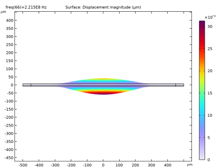
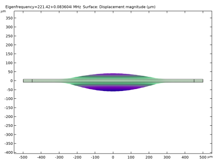
In the Settings window for Surface, click Replace Expression in the upper-right corner of the Expression section. From the menu, choose Component 1 (comp1)>Solid Mechanics>Displacement>solid.disp - Displacement magnitude - m.
3
In the Displacement (solid) toolbar, click  Plot.
4
Click the  Zoom Extents button in the Graphics toolbar.
Compare this plot with Figure 4.
Electric Potential (es) 1
1
In the Model Builder window, under Results click Electric Potential (es) 1.
2
In the Electric Potential (es) 1 toolbar, click  Plot.
Compare this plot with Figure 5.
Admittance
1
In the Home toolbar, click  Add Plot Group and choose 1D Plot Group.
2
In the Settings window for 1D Plot Group, type Admittance in the Label text field.
3
Locate the Data section. From the Dataset list, choose Study 2/Solution 2 (sol2).
Global 1
1
Right-click Admittance and choose Global.
2
In the Settings window for Global, locate the y-Axis Data section.
3
4
Locate the x-Axis Data section. From the Unit list, choose MHz.
5
In the Admittance toolbar, click  Plot.
6
Click the  y-Axis Log Scale button in the Graphics toolbar.
Compare this plot with Figure 6.
Quality Factor
1
In the Model Builder window, right-click Admittance and choose Duplicate.
2
In the Settings window for 1D Plot Group, type Quality Factor in the Label text field.
Global 1
1
In the Model Builder window, expand the Quality Factor node, then click Global 1.
2
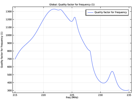
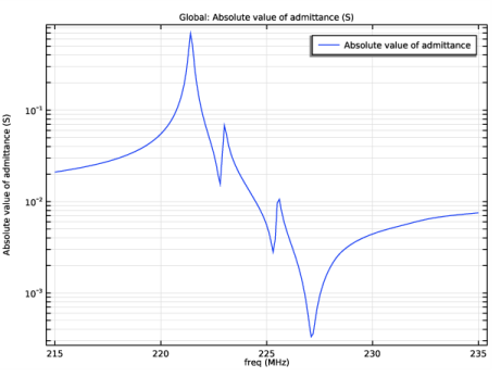
In the Settings window for Global, click Replace Expression in the upper-right corner of the y-Axis Data section. From the menu, choose Component 1 (comp1)>Solid Mechanics>Global>solid.Q_freq - Quality factor for frequency.
3
Click the  y-Axis Log Scale button in the Graphics toolbar.
4
In the Quality Factor toolbar, click  Plot.
Compare this plot with Figure 7.
The following steps show how to compute the quality factor and the decay factor for the resonance at 221.4 MHz from the eigenfrequency study. You will see that the value for the quality factor agrees well with that obtained from the frequency domain study at the same frequency.
Q Factor
1
In the Results toolbar, click  Global Evaluation.
2
In the Settings window for Global Evaluation, type Q Factor in the Label text field.
3
Locate the Data section. From the Eigenfrequency selection list, choose From list.
4
In the Eigenfrequency (MHz) list, select 221.42+0.083604i.
5
Click Replace Expression in the upper-right corner of the Expressions section. From the menu, choose Component 1 (comp1)>Solid Mechanics>Global>solid.Q_eig - Quality factor for eigenvalue.
6
Click  Evaluate.
Decay Factor
1
Right-click Q Factor and choose Duplicate.
2
In the Settings window for Global Evaluation, click Replace Expression in the upper-right corner of the Expressions section. From the menu, choose Component 1 (comp1)>Solid Mechanics>Global>solid.decay - Exponential decay factor.
3
In the Label text field, type Decay Factor.
4
Click  Evaluate.
Streamline 1
1
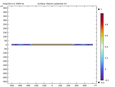
In the Model Builder window, expand the Results>Electric Potential (es) node, then click Streamline 1.
2
In the Settings window for Streamline, locate the Streamline Positioning section.
3
In the Separating distance text field, type 0.005.
4
In the Electric Potential (es) toolbar, click  Plot.
Streamline 1
1
In the Model Builder window, expand the Results>Electric Field Norm (es) node, then click Streamline 1.
2
In the Settings window for Streamline, locate the Streamline Positioning section.
3
In the Separating distance text field, type 0.005.
4
In the Electric Field Norm (es) toolbar, click  Plot.
Streamline 1
1
In the Model Builder window, expand the Results>Electric Potential (es) 1 node, then click Streamline 1.
2
In the Settings window for Streamline, locate the Streamline Positioning section.
3
In the Separating distance text field, type 0.005.
4
In the Electric Potential (es) 1 toolbar, click  Plot.
Streamline 1
1
In the Model Builder window, expand the Results>Electric Field Norm (es) 1 node, then click Streamline 1.
2
In the Settings window for Streamline, locate the Streamline Positioning section.
3
In the Separating distance text field, type 0.005.
4
In the Electric Field Norm (es) 1 toolbar, click  Plot.