You are viewing the documentation for an older COMSOL version. The latest version is available here.
PDF

Normal Modes of a Biased Resonator — 3D Geometry from a GDS-File
Introduction
When modeling a MEMS or semiconductor device with complex 3D structure, the geometry buildup can be time consuming, tedious, and error-prone. Buildup can require numerous primitive shapes in an assembly that does not correspond to how such a device would be fabricated, i.e. through sequence of processes that deposit and pattern the distinct materials one layer at a time. This tutorial demonstrates how, with the ECAD Import, and Design Modules, we can emulate semiconductor fabrication processes to build 3D geometry more efficiently and in a way that reflects actual semiconductor or MEMS fabrication.
This tutorial recreates from a GDS file the device structure modeled in the Stationary Analysis of a Biased Resonator — 3D using operations available in the ECAD Import, and Design Modules. The original model was created from 15 rectangles specified by 60 parameters. In contrast, this tutorial builds the geometry layer-by-layer and requires only 7 parameters with 6 of them for specifying thicknesses of the layers. This greatly simplifies future optimization studies.
After the geometry model is completed, the tutorial solves for the eigenmodes of the structure which can be compared to the results in the Normal Modes of a Biased Resonator — 3D.
Model Definition
The following is an outline of the steps that you can use to emulate basic MEMS or semiconductor fabrication processes using geometry operations. For the detailed instructions see the Modeling Instructions section.
Deposition of a Layer of Material over a Flat Surface
To create the geometry for a layer deposited over a flat surface, use an Import operation. Depending on the mask in GDS file, the resulting layer could be patterned or unpatterned. During the import the layer is extruded according to the specified thickness and elevation values. The substrate layer imported in this way is shown in Figure 1.
Figure 1: First layer: substrate.
The unpatterned nitride layer, imported as the second layer in the structure is shown Figure 2.
Figure 2: Second layer: nitride.
Deposition and Patterning of a Layer of Material over a Flat Surface
When a patterned layer is deposited over a flat surface, and the GDS file contains the mask for the layer when using positive photoresist, the imported layer can be directly extruded by the Import operation. The import then replicates the sequence of processes that include material deposition, photoresist coating and exposure, etching of the material, and the photoresist stripping. In the model, this is illustrated by importing layer 3 that corresponds to the polysilicon base, shown in Figure 3.
Figure 3: Third layer: the polysilicon base.
Conformal deposition of a layer of material over non-flat surface
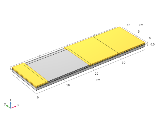
Two layers in this structure are deposited over a non-flat surface: the sacrificial layer and the polysilicon layer for the beam. You can follow the same workflow for creating both layers. The following is an overview for how to create the sacrificial layer which covers the patterned polysilicon base and the exposed parts of the nitride layer. This layer is thus to be created over a non-flat surface, so the import operation cannot be used to extrude the layer mask in one step. Instead, a sequence of geometry operations, including Offset Faces and Difference, is first used to emulate the deposition of the material. The result of these operations is shown in Figure 4.
Figure 4: The fourth sacrificial layer. This layer is conformal to the underlying polysilicon base.
Coating and patterning of virtual photoresist
The patterning of the conformal sacrificial layer can be done in two steps. First, create a virtual photoresist by importing the mask. This is equivalent to photoresist coating and lithographic patterning, as shown in Figure 5. In the subsequent step, use the Intersection operation to transfer the pattern of virtual photoresist to the target layer. The virtual photoresist layer must penetrate the entire depth of the target layer, so this determines the elevation and thickness of the imported mask layer.
Figure 5: Patterned virtual photoresist layer.
Patterning of a layer of material over non-flat surface
By using the Intersection operation, you can transfer the photoresist pattern to the target sacrificial layer. This step is equivalent to an etch process followed by a photoresist strip. What remains is the patterned sacrificial layer, as seen in Figure 6.
Figure 6: Patterned sacrificial layer.
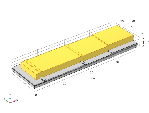
To obtain the patterned polysilicon beam deposited over the sacrificial layer and the exposed faces of the polysilicon base and nitride layers, follow the same steps as when creating the sacrificial layer. The result is shown in Figure 7.
Figure 7: Patterned polysilicon beam.
Removal of a layer of material
To remove the sacrificial layer seen in Figure 8 use the Delete Entities operation. This step is equivalent to an isotropic etch process for releasing the structure. The completed half structure is shown in Figure 9.
Figure 8: The sacrificial layer under the polysilicon beam is selected for removal.
Figure 9: Completed half of the geometry.
For this tutorial it is not enough to model half of the geometry using symmetry boundary conditions, because doing so excludes all the antisymmetric vibrational modes. The geometry is therefore mirrored prior to performing the eigenfrequency analysis.
Results and Discussion
Figure 10, Figure 11, and Figure 12 show the normal modes of the device, together with the eigenfrequencies, in the unbiased state. The lowest three normal modes are symmetric and anti-symmetric bending modes and a torsional mode. These results are similar to those in Normal Modes of a Biased Resonator — 3D.
Figure 10: Symmetric bending mode, fo = 8.4 MHz.
Figure 11: Anti-symmetric bending mode, fo = 22.3 MHz.
Figure 12: Torsional mode, fo = 27.2 MHz.
Application Library path: MEMS_Module/Actuators/biased_resonator_3d_ecad_design
Modeling Instructions
Create a 3D model with a Solid Mechanics interface.
From the File menu, choose New.
New
In the New window, click  Model Wizard.
Model Wizard
1
In the Model Wizard window, click  3D.
2
In the Select Physics tree, select Structural Mechanics>Solid Mechanics (solid).
3
Click Add.
4
Click  Study.
5
In the Select Study tree, select General Studies>Eigenfrequency.
6
Global Definitions
Enter the parameters used for creating the geometry.
Parameters 1
1
In the Model Builder window, under Global Definitions click Parameters 1.
2
In the Settings window for Parameters, locate the Parameters section.
3
Geometry 1
While it is possible to import all layers at the same time, it is easier to view the resulting 3D geometry if you import and build the layers one at a time.
1
In the Model Builder window, expand the Component 1 (comp1)>Geometry 1 node, then click Geometry 1.
2
In the Settings window for Geometry, locate the Units section.
3
From the Length unit list, choose µm.
In addition to the ECAD Import Module functionality, the Offset Faces operation, which is part of the Design Module, is used to create the geometry. Make sure that the CAD kernel is used.
4
Locate the Advanced section. From the Geometry representation list, choose CAD kernel.
Import 1 = L1, Substrate
Start with importing the substrate.
1
In the Home toolbar, click  Import.
2
In the Settings window for Import, type Import 1 = L1, Substrate in the Label text field.
3
Locate the Import section. Click  Browse.
4
5
Find the Layers to import subsection. Select the Manual control of elevations check box.
6
7
Locate the Selections of Resulting Entities section. Clear the Layer selections check box.
8
Click  Build Selected.
Import 2 = L2, Deposit Nitride Layer
Continue with creating the nitride layer. The easiest is to duplicate the previous import, then edit the settings for importing Layer 2 from the file.
1
Right-click Import 1 = L1, Substrate and choose Duplicate.
2
In the Settings window for Import, type Import 2 = L2, Deposit Nitride Layer in the Label text field.
3
Locate the Import section. Find the Layers to import subsection. In the table, enter the following settings:
4
Click  Build Selected.
5
Click  Highlight Result, for a better visualization of the result from the import.
Import 3 = L3, Deposit and Pattern Polysilicon Base Layer
Next, create the polysilicon base layer. The mask for this is Layer 3 in the GDS file. This is a patterned layer, but as it is deposited over a flat surface, you can import and extrude it in one step, just as the previous two layers.
1
Right-click Import 2 = L2, Deposit Nitride Layer and choose Duplicate.
2
In the Settings window for Import, type Import 3 = L3, Deposit and Pattern Polysilicon Base Layer in the Label text field.
3
Locate the Import section. Find the Layers to import subsection. In the table, enter the following settings:
4
Click  Build Selected.
Offset Faces 1 = Deposit Sacrificial Layer
Continue with creating the sacrificial layer, which is deposited over the polysilicon base, as well as the exposed nitride layer. Before importing the mask for the sacrificial layer, emulate its deposition by using the Offset Faces operation to offset in the normal direction the top faces of the nitride and polysilicon layers, and the exposed vertical faces of the polysilicon islands.
1
In the Geometry toolbar, click  Editing and choose Offset Faces.
2
On the object imp3, select Boundaries 1, 4–7, and 10 only.
3
On the object imp2, select Boundary 4 only.
4
In the Settings window for Offset Faces, locate the Faces section.
5
Select the Keep input objects check box.
6
Locate the Offset section. In the Distance text field, type t_sl.
7
In the Label text field, type Offset Faces 1 = Deposit Sacrificial Layer.
8
Click  Build Selected.
Offsetting the faces created larger copies of the nitride and polysilicon objects, while also keeping the original objects for these layers, since the Keep input objects check box is selected. To obtain only the sacrificial layer as one object, use a Difference operation to remove the objects for the nitride and polysilicon layers from the objects resulting from the offset.
Difference 1 = Deposit Sacrificial Layer
1
In the Geometry toolbar, click  Booleans and Partitions and choose Difference.
2
In the Settings window for Difference, type Difference 1 = Deposit Sacrificial Layer in the Label text field.
3
Select the objects off1(1) and off1(2) only.
4
Locate the Difference section. Find the Objects to subtract subsection. Click to select the  Activate Selection toggle button.
5
Select the objects imp2 and imp3 only.
6
Select the Keep objects to subtract check box.
7
Clear the Keep interior boundaries check box.
8
Click  Build Selected.
Next, import the mask for the sacrificial layer, which is Layer 4 in the GDS file.
Import 4 = L4, Pattern Sacrificial Layer
1
In the Model Builder window, under Component 1 (comp1)>Geometry 1 right-click Import 3 = L3, Deposit and Pattern Polysilicon Base Layer (imp3) and choose Duplicate.
2
In the Settings window for Import, type Import 4 = L4, Pattern Sacrificial Layer in the Label text field.
3
Locate the Import section. Find the Layers to import subsection. In the table, enter the following settings:
4
Click  Build Selected.
Intersection 1 = L4, Pattern Sacrificial Layer
To create the patterned sacrificial layer, intersect the extruded mask layer, resulting from Import 4, with the sacrificial layer that resulted from the Difference 1 operation. This step emulates the sacrificial layer etch followed by a photoresist strip.
1
In the Geometry toolbar, click  Booleans and Partitions and choose Intersection.
2
In the Settings window for Intersection, type Intersection 1 = L4, Pattern Sacrificial Layer in the Label text field.
3
Select the objects dif1 and imp4 only.
4
Locate the Intersection section. Clear the Keep interior boundaries check box.
5
Click  Build Selected.
The layer for the polysilicon beam is patterned and deposited over the sacrificial layer, and the exposed faces of the polysilicon base and nitride layers. To create this layer apply the same steps as when creating the sacrificial layer. Continue with offsetting the top faces of the sacrificial, polysilicon base and nitride layers.
Offset Faces 2 = Deposit Polysilicon Layer
1
In the Geometry toolbar, click  Editing and choose Offset Faces.
2
In the Settings window for Offset Faces, type Offset Faces 2 = Deposit Polysilicon Layer in the Label text field.
3
On the object imp2, select Boundary 4 only.
4
On the object imp3, select Boundary 4 only.
5
On the object int1, select Boundaries 4, 9, 18, 22, and 31 only.
6
Locate the Offset section. In the Distance text field, type t_poly.
7
Locate the Faces section. Select the Keep input objects check box.
8
Click  Build Selected.
Difference 2 = Deposit Polysilicon Layer
1
In the Geometry toolbar, click  Booleans and Partitions and choose Difference.
2
In the Settings window for Difference, type Difference 2 = Deposit Polysilicon Layer in the Label text field.
3
Select the objects off2(1), off2(2), and off2(3) only.
4
Locate the Difference section. Find the Objects to subtract subsection. Click to select the  Activate Selection toggle button.
5
Select the objects int1, imp2, and imp3 only.
6
Select the Keep objects to subtract check box.
7
Clear the Keep interior boundaries check box.
8
Click  Build Selected.
Import 5 = L5, Pattern Polysilicon Layer
1
In the Model Builder window, under Component 1 (comp1)>Geometry 1 right-click Import 4 = L4, Pattern Sacrificial Layer (imp4) and choose Duplicate.
2
In the Settings window for Import, type Import 5 = L5, Pattern Polysilicon Layer in the Label text field.
3
Locate the Import section. Find the Layers to import subsection. In the table, enter the following settings:
4
Click  Build Selected.
Intersection 2 = Pattern Polysilicon Layer
1
In the Geometry toolbar, click  Booleans and Partitions and choose Intersection.
2
In the Settings window for Intersection, type Intersection 2 = Pattern Polysilicon Layer in the Label text field.
3
Select the objects dif2 and imp5 only.
4
Locate the Intersection section. Clear the Keep interior boundaries check box.
5
Click  Build Selected.
To obtain the final geometry, delete the object for the sacrificial layer. This step emulates an isotropic oxide etch to release the polysilicon beam.
Delete Entities 1 (del1)
1
In the Model Builder window, right-click Geometry 1 and choose Delete Entities.
2
In the Settings window for Delete Entities, locate the Entities or Objects to Delete section.
3
From the Geometric entity level list, choose Object.
4
5
Click  Build Selected.
Define named selections for the layers.
Explicit Selection 1 = Polysilicon Beam
1
In the Geometry toolbar, click  Selections and choose Explicit Selection.
2
On the object imp3, select Domain 1 only.
3
On the object int2, select Domain 1 only.
4
In the Settings window for Explicit Selection, type Explicit Selection 1 = Polysilicon Beam in the Label text field.
5
Click  Build Selected.
Explicit Selection 2 = Bottom Electrode
1
In the Geometry toolbar, click  Selections and choose Explicit Selection.
2
On the object imp3, select Domain 2 only.
3
In the Settings window for Explicit Selection, type Explicit Selection 2 = Bottom Electrode in the Label text field.
4
Click  Build Selected.
Explicit Selection 3 = Nitride
1
In the Geometry toolbar, click  Selections and choose Explicit Selection.
2
In the Settings window for Explicit Selection, type Explicit Selection 3 = Nitride in the Label text field.
3
On the object imp2, select Domain 1 only.
4
Click  Build Selected.
Explicit Selection 4 = Substrate
1
In the Geometry toolbar, click  Selections and choose Explicit Selection.
2
In the Settings window for Explicit Selection, type Explicit Selection 4 = Substrate in the Label text field.
3
On the object imp1, select Domain 1 only.
4
Click  Build Selected.
Finally, mirror the geometry so that asymmetric eigenmodes can be calculated.
Mirror 1 (mir1)
1
In the Geometry toolbar, click  Transforms and choose Mirror.
2
Click in the Graphics window and then press Ctrl+A to select all objects.
3
In the Settings window for Mirror, locate the Point on Plane of Reflection section.
4
In the x text field, type w_box.
5
Locate the Normal Vector to Plane of Reflection section. In the x text field, type 1.
6
In the z text field, type 0.
7
Locate the Input section. Select the Keep input objects check box.
8
Click  Build Selected.
Add Material
1
In the Home toolbar, click  Add Material to open the Add Material window.
2
Go to the Add Material window.
3
In the tree, select MEMS>Semiconductors>Si - Polycrystalline silicon.
4
Click Add to Component in the window toolbar.
5
In the tree, select MEMS>Insulators>Si3N4 - Silicon nitride.
6
Click Add to Component in the window toolbar.
7
In the tree, select MEMS>Insulators>SiO2 - Silicon oxide.
8
Click Add to Component in the window toolbar.
9
In the Home toolbar, click  Add Material to close the Add Material window.
Materials
Si3N4 - Silicon nitride (mat2)
1
In the Model Builder window, under Component 1 (comp1)>Materials click Si3N4 - Silicon nitride (mat2).
2
In the Settings window for Material, locate the Geometric Entity Selection section.
3
From the Selection list, choose Explicit Selection 3 = Nitride.
SiO2 - Silicon oxide (mat3)
1
In the Model Builder window, click SiO2 - Silicon oxide (mat3).
2
In the Settings window for Material, locate the Geometric Entity Selection section.
3
From the Selection list, choose Explicit Selection 4 = Substrate.
Solid Mechanics (solid)
1
In the Model Builder window, under Component 1 (comp1) click Solid Mechanics (solid).
2
3
In the Settings window for Solid Mechanics, locate the Domain Selection section.
4
From the Selection list, choose Explicit Selection 1 = Polysilicon Beam.
Fixed Constraint 1
1
In the Physics toolbar, click  Domains and choose Fixed Constraint.
2
Mesh 1
In the Model Builder window, under Component 1 (comp1) right-click Mesh 1 and choose Build All.
Study 1
Step 1: Eigenfrequency
1
In the Model Builder window, under Study 1 click Step 1: Eigenfrequency.
2
In the Settings window for Eigenfrequency, locate the Study Settings section.
3
Select the Desired number of eigenfrequencies check box. In the associated text field, type 3.
4
In the Home toolbar, click  Compute.
Results
Mode Shape (solid)
In the Model Builder window, expand the Results>Mode Shape (solid) node.
Surface 1
1
In the Model Builder window, expand the Results>Mode Shape (solid)>Surface 1 node, then click Surface 1.
2
In the Settings window for Surface, locate the Coloring and Style section.
3
Click  Change Color Table.
4
In the Color Table dialog box, select Rainbow>Rainbow in the tree.
5
6
Click the  Zoom Extents button in the Graphics toolbar.
7
In the Settings window for Surface, click  Plot Next.
8
Click  Plot Next.