PDF

Electrical Heating in a Busbar Assembly
Introduction
This tutorial analyzes the anode to busbar coupling designed to conduct a direct current from a current source to the anode in an electrolysis process, such as the chlor-alkali process for the production of chlorine and sodium. The current that passes from the intercell busbar to the anode produces heat due to the resistive losses, a phenomenon referred to as Joule heating. The Joule heating effect is described by conservation laws for electric current and energy. Once solved for, the two conservation laws give the temperature and electric field, respectively.
The geometry for the simulation, displayed in Figure 1, includes the coupling components for one cell, and a section of the intercell busbar that is connected to the power source. It consists of the top of the anode with four central columns holding copper rods attached to copper bars.
Figure 1: The geometry of the anode to busbar coupling used in this example.
When designing the coupling to the busbar it is important to aim for a low operational temperature for the copper components to avoid excessive oxidation and to maintain a high electrical conductivity. The goal of your simulation is to precisely calculate how much the busbar heats up, and to study the influence of two design parameters, the diameter of the rods rising from the top of the anode and the width of the copper connectors that link to the intercell busbar, on the phenomenon. By conducting a parametric sweep you can determine which combinations of these parameters result in a maximum temperature in the copper components that is less than 90°C. Above this temperature the oxidation rate of copper starts to increase.
Model Definition
The intercell busbar, the various connector bars, and the rods rising from the anode are made of copper. For the components of the anode and the bolts that hold the copper busbars together, we choose titanium assuming a highly corrosive environment.
All surfaces, except the anode bottom surface in contact with the electrolyte and the grounded surfaces of the intercell busbar, are cooled by natural convection in the air surrounding the busbar. We use the convective heat flux boundary condition for the purpose, assuming a cell room temperature of to 35°C. The same boundary condition is applied at the bottom surface of the anode, where the temperature of the surrounding electrolyte is set to 100°C. The intercell busbar cross section boundaries do not contribute to cooling or heating of the device. The electric potential at these boundaries is 0 V. At the bottom surface of the anode the normal current density is set to 8,000 A/m2.
Figure 2: Boundary settings in the model.
Results and Discussion
The plot shown in Figure 3 displays the temperature in the device, which is substantially higher than the ambient temperature 35°C. The highest temperature is experienced by the titanium parts in contact with the hot electrolyte. For the copper components, the temperature variation is largest in the copper rods.
Figure 3: Temperature distribution in the busbar.
The temperature distribution is symmetric with a vertical mirror plane running through the anode at a right angle to the intercell busbar. In this case, the model does not require much computing power and you can model the whole geometry. For more complex models, you should consider using symmetries in order to reduce the size of the model.
Increasing the diameter of the copper rod and the width of the connector rods, while keeping the applied current density constant, leads to a lower temperature in the device. While the increased cross-sectional area leads to more heat produced by resistive losses, there is an even larger increase in the cooling effect as the total surface area increases, resulting in the lowering of the temperature.
By plotting the maximum temperature in the copper components against the diameter and width parameters, and formatting the plot according to Figure 4, we can easily determine the combinations of the diameter and width parameters that lead to an acceptable value of the maximum temperature.
Figure 4: Maximum temperature in the busbar assembly plotted against the rod diameter and the connector width parameters, and formatted to show the parameter combinations that lead to a maximum temperature of less than 90°C.
Notes About the COMSOL Implementation
The busbar geometry you are using in this example comes from an Inventor assembly. The LiveLink interface transfers the geometry from Inventor to COMSOL Multiphysics. Using the interface you are also able to update the dimensions of the busbar in the Inventor file. In order for this to work you need to have both programs running during modeling, and you need to make sure that the busbar assembly file is the active file in Inventor.
Application Library path: LiveLink_for_Inventor/Tutorials,_LiveLink_Interface/busbar_llinventor
Modeling Instructions
You can set up this simulation both by working inside Inventor, using the embedded COMSOL simulation environment, and by working in the standalone COMSOL Desktop. Regardless which way you proceed, first you need to open the CAD file with the geometry in Inventor.
1
In Inventor open the file busbar_assembly_cad/busbar_assembly.iam located in the model’s Application Library folder.
2
Modeling Inside Inventor
1
On the COMSOL Multiphysics tab click the New button.
In case it is not already running, the COMSOL modeling environment will be started, and the geometry will be synchronized automatically.
2
COMSOL Desktop
From the File menu, choose New.
New
In the New window, click  Model Wizard.
Model Wizard
1
In the Model Wizard window, click  3D.
2
In the Select Physics tree, select Heat Transfer>Electromagnetic Heating>Joule Heating.
3
Click Add.
4
Click  Study.
5
In the Select Study tree, select General Studies>Stationary.
6
Geometry 1
The geometry is already synchronized if you are modeling inside Inventor, and you can skip to step 4 in the section LiveLink for Inventor 1 (cad1).
Make sure that the CAD Import Module kernel is used.
1
In the Model Builder window, under Component 1 (comp1) click Geometry 1.
2
In the Settings window for Geometry, locate the Advanced section.
3
From the Geometry representation list, choose CAD kernel.
LiveLink for Inventor 1 (cad1)
1
Right-click Component 1 (comp1)>Geometry 1 and choose LiveLink Interfaces>LiveLink for Inventor.
2
In the Settings window for LiveLink for Inventor, locate the Synchronize section.
3
Click Synchronize.
After a few moments the geometry of the busbar assembly appears in the Graphics window.
4
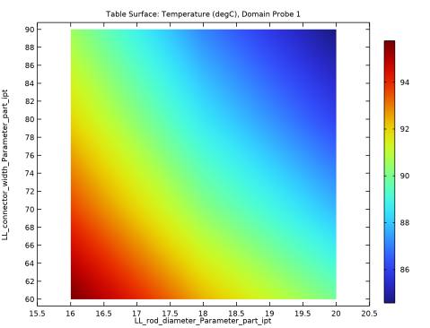
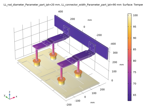
Click to expand the Parameters in CAD Package section. The table contains the two dimensions, rod_diameter.Parameter_part.ipt and connector_width.Parameter_part.ipt, which are part of the Inventor model. In Inventor, the Parameter Selection button on the COMSOL Multiphysics tab allows you to select and view dimensions for synchronization. These dimensions are retrieved, and appear in the CAD name column of the table. The corresponding entries in the COMSOL name column, LL_rod_diameter_Parameter_part_ipt and LL_connector_width_Parameter_part_ipt, are global parameters in the COMSOL model. These are automatically generated during synchronization, and are assigned the values of the linked Inventor dimensions. The parameter values are displayed in the COMSOL value column.
Global parameters in a model allow you to parameterize settings and can be controlled by the parametric solver to perform parametric sweeps. Thus, by linking Inventor dimensions to COMSOL global parameters, the parametric solver can automatically update and synchronize the geometry for each new value in a sweep.
5
Click to expand the Object Selections section. The selections displayed here are automatically generated based on the assigned materials in the Inventor components.
6
Click to expand the Boundary Selections section. The selections listed here are user defined selections saved in the Inventor files for the components that they appear on. In Inventor, you can set-up selections using the Selections button on the COMSOL Multiphysics tab.
Skip the next step if you are working in the embedded COMSOL simulation environment inside Inventor.
7
Right-click LiveLink for Inventor 1 (cad1) and choose Build All.
Adjacent Selection 1 (adjsel1)
1
In the Model Builder window, right-click Geometry 1 and choose Selections>Adjacent Selection.
2
In the Settings window for Adjacent Selection, locate the Input Entities section.
3
4
In the Add dialog box, in the Input selections list, choose Copper and Titanium.
5
6
In the Settings window for Adjacent Selection, locate the Resulting Selection section.
7
From the Show in physics list, choose Off.
Heat flux boundaries
1
Right-click Geometry 1 and choose Selections>Difference Selection.
2
In the Settings window for Difference Selection, type Heat flux boundaries in the Label text field.
3
Locate the Geometric Entity Level section. From the Level list, choose Boundary.
4
Locate the Input Entities section. Click  Add.
5
In the Add dialog box, select Adjacent Selection 1 in the Selections to add list.
6
7
In the Settings window for Difference Selection, locate the Input Entities section.
8
9
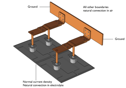
In the Add dialog box, in the Selections to subtract list, choose Electrolyte boundary and Grounded boundaries.
10
Global Definitions
Parameters 1
The table already contains the automatically generated global parameters that are linked to the Inventor dimensions. It is possible to edit the values of these parameters here, and then synchronize, to modify the geometry. But here we will use the parametric solver to modify the parameters.
Continue with loading additional parameters for setting up the physics.
1
In the Model Builder window, under Global Definitions click Parameters 1.
2
In the Settings window for Parameters, locate the Parameters section.
3
Click  Load from File.
4
Materials
Add Material
From the Home menu, choose Add Material.
Add Material
1
Go to the Add Material window.
2
In the tree, select Built-in>Copper.
3
Click Add to Component in the window toolbar.
Materials
Copper (mat1)
1
In the Settings window for Material, locate the Geometric Entity Selection section.
2
From the Selection list, choose Copper.
Add Material
1
Go to the Add Material window.
2
In the tree, select Built-in>Titanium beta-21S.
3
Click Add to Component in the window toolbar.
Add Material
1
From the Home menu, choose Add Material.
2
In the Settings window for Material, locate the Geometric Entity Selection section.
3
From the Selection list, choose Titanium.
Electric Currents (ec)
Ground 1
1
In the Model Builder window, under Component 1 (comp1) right-click Electric Currents (ec) and choose Ground.
2
In the Settings window for Ground, locate the Boundary Selection section.
3
From the Selection list, choose Grounded boundaries.
Normal Current Density 1
1
In the Model Builder window, right-click Electric Currents (ec) and choose Normal Current Density.
2
In the Settings window for Normal Current Density, locate the Boundary Selection section.
3
From the Selection list, choose Electrolyte boundary.
4
Locate the Normal Current Density section. In the Jn text field, type Jan.
Heat Transfer in Solids (ht)
Heat Flux 1
1
In the Model Builder window, under Component 1 (comp1) right-click Heat Transfer in Solids (ht) and choose Heat Flux.
2
In the Settings window for Heat Flux, locate the Boundary Selection section.
3
From the Selection list, choose Heat flux boundaries.
4
Locate the Heat Flux section. From the Flux type list, choose Convective heat flux.
5
In the h text field, type htca.
6
In the Text text field, type Ta.
Heat Flux 2
1
In the Model Builder window, right-click Heat Transfer in Solids (ht) and choose Heat Flux.
2
In the Settings window for Heat Flux, locate the Boundary Selection section.
3
From the Selection list, choose Electrolyte boundary.
4
Locate the Heat Flux section. From the Flux type list, choose Convective heat flux.
5
In the h text field, type htce.
6
In the Text text field, type Te.
Mesh 1
1
In the Model Builder window, under Component 1 (comp1) click Mesh 1.
2
In the Settings window for Mesh, locate the Sequence Type section.
3
From the list, choose User-controlled mesh.
Size
1
In the Model Builder window, under Component 1 (comp1)>Mesh 1 click Size.
2
In the Settings window for Size, locate the Element Size section.
3
Click the Custom button.
4
Locate the Element Size Parameters section. In the Minimum element size text field, type mh.
5
Click  Build All.
Study 1
Parametric Sweep
1
In the Model Builder window, right-click Study 1 and choose Parametric Sweep.
2
In the Settings window for Parametric Sweep, locate the Study Settings section.
3
4
From the list in the Parameter name column, choose LL_rod_diameter_Parameter_part_ipt.
5
Click  Range.
6
In the Range dialog box, type 16[mm] in the Start text field.
7
In the Step text field, type 2[mm].
8
In the Stop text field, type 20[mm].
9
Click Replace.
10
In the Parameter unit column, enter mm.
11
In the Settings window for Parametric Sweep, locate the Study Settings section.
12
13
14
From the list in the Parameter name column, choose LL_connector_width_Parameter_part_ipt.
15
Click  Range.
16
In the Range dialog box, type 60[mm] in the Start text field.
17
In the Step text field, type 10[mm].
18
In the Stop text field, type 90[mm].
19
Click Replace.
20
In the Parameter unit column, enter mm.
As the last step before computing the solution, configure the sweep to include all combinations of the two parameters.
21
In the Settings window for Parametric Sweep, locate the Study Settings section.
22
From the Sweep type list, choose All combinations.
Solution 1 (sol1)
1
Right-click Study 1 and choose Show Default Solver.
2
In the Model Builder window, expand the Solution 1 (sol1) node.
3
In the Model Builder window, expand the Study 1>Solver Configurations>Solution 1 (sol1)>Stationary Solver 1 node, then click Segregated 1.
4
In the Settings window for Segregated, locate the General section.
5
From the Stabilization and acceleration list, choose Anderson acceleration.
6
Right-click Study 1>Solver Configurations>Solution 1 (sol1)>Stationary Solver 1>Segregated 1 and choose Compute.
Results
Temperature (ht)
1
In the Settings window for 3D Plot Group, locate the Plot Settings section.
2
From the Color list, choose Gray.
Surface
1
In the Model Builder window, expand the Temperature (ht) node, then click Surface.
2
In the Settings window for Surface, locate the Expression section.
3
From the Unit list, choose degC.
4
Locate the Coloring and Style section. Click  Change Color Table.
5
In the Color Table dialog box, select Thermal>HeatCameraLight in the tree.
6
7
In the Settings window for Surface, click  Plot.
You should now see a plot similar to the one in Figure 3.
Definitions
Add a domain probe to calculate the average temperature increase from ambient temperature in the device.
Domain Probe 1 (dom1)
1
In the Model Builder window, under Component 1 (comp1) right-click Definitions and choose Probes>Domain Probe.
2
In the Settings window for Domain Probe, locate the Probe Type section.
3
From the Type list, choose Maximum.
4
Locate the Source Selection section. From the Selection list, choose Copper.
5
Click Replace Expression in the upper-right corner of the Expression section. From the menu, choose Component 1 (comp1)>Heat Transfer in Solids>Temperature>T - Temperature - K.
6
Locate the Expression section. From the Table and plot unit list, choose degC.
7
Click  Update Results.
Table
1
Go to the Table window.
2
Click Table Surface in the window toolbar.
A plot similar to the one displayed below appears.
Results
In the last few steps you can add annotations and format the plot to make it easier to read which parameter combinations result in an accepted temperature increase.
Table Surface 2
1
In the Model Builder window, under Results>2D Plot Group 6 right-click Table Surface 1 and choose Duplicate.
2
In the Settings window for Table Surface, click to expand the Title section.
3
From the Title type list, choose None.
4
Click to expand the Range section. Select the Manual data range check box.
5
In the Maximum text field, type 90.
6
Locate the Coloring and Style section. From the Coloring list, choose Uniform.
7
From the Color list, choose Green.
Table Surface 1
1
In the Model Builder window, click Table Surface 1.
2
In the Settings window for Table Surface, locate the Range section.
3
Select the Manual data range check box.
4
In the Minimum text field, type 90.
5
Locate the Coloring and Style section. From the Coloring list, choose Uniform.
2D Plot Group 6
1
In the Model Builder window, click 2D Plot Group 6.
2
In the Settings window for 2D Plot Group, locate the Plot Settings section.
3
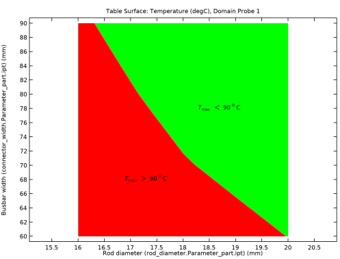
Select the x-axis label check box. In the associated text field, type Rod diameter (rod_diameter.Parameter_part.ipt) (mm).
4
Select the y-axis label check box. In the associated text field, type Busbar width (connector_width.Parameter_part.ipt) (mm).
Annotation 1
1
Right-click 2D Plot Group 6 and choose Annotation.
2
In the Settings window for Annotation, locate the Data section.
3
From the Dataset list, choose Domain Probe 1.
4
Locate the Annotation section. In the Text text field, type $T_\max\ >\ 90 \degree \mathrm{C}$.
5
Locate the Position section. In the x text field, type 16.8[mm].
6
In the y text field, type 69[mm].
7
Locate the Annotation section. Select the LaTeX markup check box.
8
Locate the Coloring and Style section. Clear the Show point check box.
Annotation 2
1
Right-click 2D Plot Group 6 and choose Annotation.
2
In the Settings window for Annotation, locate the Data section.
3
From the Dataset list, choose Domain Probe 1.
4
Locate the Annotation section. In the Text text field, type $T_\max\ <\ 90 \degree \mathrm{C}$.
5
Locate the Position section. In the x text field, type 18.2[mm].
6
In the y text field, type 79[mm].
7
Locate the Annotation section. Select the LaTeX markup check box.
8
Locate the Coloring and Style section. Clear the Show point check box.
9
The plot in the Graphics window should now look similar to the one in Figure 4.