PDF

Heating Circuit: Layered Shell Version
Introduction
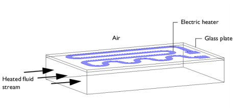
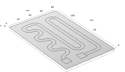
Small heating circuits find use in many applications. For example, in manufacturing processes they heat up reactive fluids. Figure 1 illustrates a typical heating device shown in this model. The device consists of an electrically resistive layer deposited on a glass plate. The layer causes Joule heating when a voltage is applied to the circuit. The layer’s properties determine the amount of heat produced.
Figure 1: Geometry of a heating device.
In this particular model, there are three important design considerations:
The heater must also work without failure. The first and second requirements are achieved by inserting a glass plate between the heating circuit and the fluid; it acts as a conducting separator. Glass is an ideal material for both these purposes because it is nonreactive and has a low coefficient of thermal expansion.
Overheating must be avoided due to the risk of self-ignition of the reactive fluid stream. Ignition is also the main reason for separating the electrical circuit from direct contact with the fluid. Heating devices are tailored for each application, making virtual prototyping very important for manufacturers.
For heating circuits in general, the detachment of the resistive layer often determines the failure rate. This is caused by excessive thermally induced interfacial stresses. Once the layer has detached, it gets locally overheated, which further accelerates the detachment. Finally, in the worst case, the circuit might overheat and burn. From this perspective, it is also important to study the interfacial tension due to the different thermal-expansion coefficients of the resistive layer and the substrate as well as the differences in temperature. The geometric shape of the layer is a key parameter to design circuits for proper functioning. You can investigate all of the abovementioned aspects by modeling the circuit.
This multiphysics example simulates the electrical heat generation, the heat transfer, and the mechanical stresses and deformations of a heating circuit device. The model uses the Heat Transfer in Shells interface of the Heat Transfer Module in combination with the Electric Currents, Layered Shell interface from the AC/DC Module and the Layered Shell interface from the Composite Materials Module.
Note: This model is a layered shell version of the heating_circuit model and requires the AC/DC Module, Heat Transfer Module, Structural Mechanics Module, and Composite Materials Module.
Model Definition
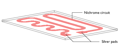
Figure 2 shows a drawing of the modeled heating circuit.
Figure 2: Drawing of the heating circuit deposited on a glass plate.
The device consists of a serpentine-shaped Nichrome resistive layer, 10 μm thick and 5 mm wide, deposited on a glass plate. At each end, it has a silver contact pad measuring 10 mm-by-10 mm-by-10 μm. When the circuit is in use, the deposited side of the glass plate is in contact with surrounding air, and the back side is in contact with the heated fluid. Assume that the edges and sides of the glass plate are thermally insulated.
Table 1 lists the resistor’s dimensions.
Table 1: Dimensions.
Layered Shell Approach
Since this model uses a layered shell interface, in which the through thickness integration is inherent to the layered shell formulation itself, a surface geometry as shown in the Figure 3 is sufficient.
Figure 3: Layered shell version of the model geometry.
The layered shell geometry has many zones with layers of different materials and thicknesses. The spatial position of the different zones can be seen in Figure 4 and material and thicknesses for each zone can be seen in Figure 5.
The different zones of the layered shell are by default disconnected. Therefore, continuity conditions connecting layers from neighboring zones are required in all physics interfaces.
Figure 4: Zones with different layers in the layered shell geometry. The green zone has only glass layer, the red zone has glass and Nichrome layers, and yellow zone has glass and Silver layers.
Figure 5: The cross sectional view of zones having layers of different material and thickness.
Boundary Conditions
During operation the resistive layer produces heat. Model the electrically generated heat using the Electric Currents, Layered Shell interface from the AC/DC Module. An electric potential of 12 V is applied to the pads. In the model, you achieve this effect by setting the potential at one edge of the first pad to 12 V, and that of one edge of the other pad to 0 V.
To model the heat transfer in the thin conducting layer, use the Heat Transfer in Shells interface. The heat rate per unit area (measured in W/m2) produced inside the thin layer is given by
(1)
where QDC = J · E = σ|∇tV|2 (W/m3) is the power density. The generated heat appears as an inward heat flux at the surface of the glass plate.
At steady state, the resistive layer dissipates the heat it generates in two ways: on its upside to the surrounding air (at 293 K), and on its downside to the glass plate. The glass plate is similarly cooled in two ways: on its circuit side by air, and on its back side by a process fluid (353 K). You model the heat fluxes to the surroundings using heat transfer coefficients, h. For the heat transfer to air, h = 5 W/(m2·K), representing natural convection. On the glass plate’s back side, h = 20 W/(m2·K), representing convective heat transfer to the fluid. The sides of the glass plate are insulated.
The model simulates thermal expansion using static structural-mechanics analyses. It uses the Layered Shell interface for the glass plate as well as for the circuit layer. The stresses are set to zero at 293 K. You determine the boundary conditions for the Layered Shell interface by adding a rigid motion suppression node and restricting all rigid body modes.
Material Properties
Table 2 summarizes the material properties used in the model.
E [GPa]
ν
α [1/K]
k [W/(m·K)]
ρ [kg/m3]
Cp [J/(kg·K)]
Results and Discussion
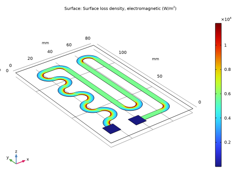
Figure 6 shows the heat that the resistive layer generates.
Figure 6: Stationary heat generation in the resistive layer when 12 V is applied.
The highest heating power occurs at the inner corners of the curves due to the higher current density at these spots. The total generated heat, as calculated by integration, is approximately 13.8 W.
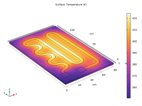
Figure 7 shows the temperature of the resistive layer and the glass plate at steady state.
Figure 7: Temperature distribution in the heating device at steady state.
The highest temperature is approximately 428 K, and it appears in the central section of the circuit layer. Interestingly, the temperature differences between the fluid side and the circuit side of the glass plate are quite small because the plate is very thin. Using boundary integration, the integral heat flux on the fluid side evaluates to approximately 8.5 W. This means that the device transfers the majority of the heat it generates — 8.5 W out of 13.8 W — to the fluid, which is good from a design perspective, although the thermal resistance of the glass plate results in some losses.
The temperature rise also induces thermal stresses due the materials’ different coefficients of thermal expansion. As a result, mechanical stresses and deformations arise in the layer and in the glass plate. Figure 8 and Figure 9 shows the effective stress distribution in the device and the resulting deformations. During operation, the glass plate bends toward the air side.
Figure 8: The thermally induced von Mises stress plotted with the deformation in glass plate.
The highest effective stress, approximately 26 MPa, occurs at the inner corners of the curves of the Nichrome circuit. The yield stress for high quality glass is roughly 250 MPa, and for Nichrome it is 360 MPa. This means that the individual objects remain structurally intact for the simulated heating power loads.
Stresses in the interface between the resistive layer and the glass plate must also be considered. Assume that the yield stress of the surface adhesion in the interface is in the region of 50 MPa — a value significantly lower than the yield stresses of the other materials in the device. If the effective stress increases above this value, the resistive layer locally detaches from the glass. Once it has detached, heat transfer is locally impeded, which can lead to overheating of the resistive layer and eventually cause the device to fail.
Figure 9: The thermally induced von Mises stress plotted with the deformation in resistive layer.
Figure 10 displays the effective forces acting on the adhesive layer during heater operation. As the figure shows, the device experiences a maximum interfacial stress that is approximately five times smaller than the yield stress. This means that the device is safe in terms of the adhesive stress.
Finally, the device’s deflections as shown in Figure 11 are studied. The maximum deviation from being a planar surface, is approximately 50 μm. For high-precision applications, such as semiconductor processing, this might be a significant value that limits the device’s operating temperature.
Figure 10: The effective forces in the interface between the resistive layer and the glass plate.
Figure 11: Deviation from a plane surface on the fluid side of the glass plate.
Application Library path: Composite_Materials_Module/Multiphysics/heating_circuit_layered
Modeling Instructions
From the File menu, choose New.
New
In the New window, click  Model Wizard.
Model Wizard
1
In the Model Wizard window, click  3D.
2
In the Select Physics tree, select Structural Mechanics>Thermal-Structure Interaction>Thermal Stress, Layered Shell.
3
Click Add.
4
In the Select Physics tree, select AC/DC>Electric Fields and Currents>Electric Currents in Layered Shells (ecis).
5
Click Add.
6
Click  Study.
7
In the Select Study tree, select General Studies>Stationary.
8
The Thermal Stress, Layered Shell interface includes the Heat Transfer in Shells and the Layered Shell interfaces. In the silica glass, these two interfaces solve for temperature and displacements, respectively. In the conducting layer representing the circuit, the temperature, electrical potential, and displacement are solved by Heat Transfer In Shells, Electric Currents in Layered Shell, and the Layered Shell interfaces.
Global Definitions
Parameters 1
Load the parameters from a file.
1
In the Model Builder window, under Global Definitions click Parameters 1.
2
In the Settings window for Parameters, locate the Parameters section.
3
Click  Load from File.
4
If you do not want to build the geometry manually, you can load the geometry sequence from the stored model. In the Model Builder window, under Component 1 (comp1) right-click Geometry 1 and choose Insert Sequence. Browse to the model’s Application Libraries folder and double-click the file heating_circuit_layered.mph. You can then continue to the Definitions section below.
To build the geometry from scratch, continue here.
Geometry 1
1
In the Model Builder window, under Component 1 (comp1) click Geometry 1.
2
In the Settings window for Geometry, locate the Units section.
3
From the Length unit list, choose mm.
Work Plane 1 (wp1)
1
In the Geometry toolbar, click  Work Plane.
2
In the Settings window for Work Plane, click  Show Work Plane.
Work Plane 1 (wp1)>Plane Geometry
1
In the Model Builder window, click Plane Geometry.
2
Click the  Zoom Extents button in the Graphics toolbar.
Work Plane 1 (wp1)>Square 1 (sq1)
1
In the Work Plane toolbar, click  Square.
2
In the Settings window for Square, locate the Size section.
3
In the Side length text field, type 10.
4
Locate the Position section. In the xw text field, type 7.
5
In the yw text field, type 10.
6
Click  Build Selected.
Work Plane 1 (wp1)>Square 2 (sq2)
1
Right-click Component 1 (comp1)>Geometry 1>Work Plane 1 (wp1)>Plane Geometry>Square 1 (sq1) and choose Duplicate.
2
In the Settings window for Square, locate the Position section.
3
In the xw text field, type 30.
4
In the yw text field, type 8.
5
Click  Build Selected.
Work Plane 1 (wp1)>Polygon 1 (pol1)
1
In the Work Plane toolbar, click  Polygon.
2
In the Settings window for Polygon, locate the Coordinates section.
3
From the Data source list, choose File.
4
Click  Browse.
5
6
Click  Build Selected.
Work Plane 1 (wp1)>Fillet 1 (fil1)
1
In the Work Plane toolbar, click  Fillet.
2
On the object pol1, select Points 2–8, 23–29, 34, 36, 37, 41, and 42 only.
It might be easier to select the points by using the Selection List window. To open this window, navigate to the Home toolbar, click Windows, and choose Selection List. (If you are running the cross-platform desktop, you find Windows in the main menu.)
3
In the Settings window for Fillet, locate the Radius section.
4
In the Radius text field, type 10.
5
Click  Build Selected.
Work Plane 1 (wp1)>Fillet 2 (fil2)
1
In the Work Plane toolbar, click  Fillet.
2
On the object fil1, select Points 6–12, 26–31, 37, 40, 43, 46, 49, and 50 only.
3
In the Settings window for Fillet, locate the Radius section.
4
In the Radius text field, type 5.
5
Click  Build Selected.
Work Plane 1 (wp1)>Rectangle 1 (r1)
1
In the Work Plane toolbar, click  Rectangle.
2
In the Settings window for Rectangle, locate the Size and Shape section.
3
In the Width text field, type 80.
4
In the Height text field, type 130.
5
In the Work Plane toolbar, click  Build All.
Form Union (fin)
1
In the Home toolbar, click  Build All.
The geometry should look like the figure below.
The absolute displacement of the glass plate is not important in itself, since it is just a function of how the rigid body constraints are applied. Instead, you want to see how much the boundary deviates from being planar. To display the deviation, create a linear approximation to the deformation using a least-squares fit. Add the following nodes in order to create the required variables.
Definitions
Integration 1 (intop1)
1
In the Definitions toolbar, click  Nonlocal Couplings and choose Integration.
2
In the Settings window for Integration, type intBelow in the Operator name text field.
3
Locate the Source Selection section. From the Geometric entity level list, choose Boundary.
4
From the Selection list, choose All boundaries.
5
Locate the Advanced section. From the Frame list, choose Material  (X, Y, Z).
Variables 1
1
In the Model Builder window, right-click Definitions and choose Variables.
2
In the Settings window for Variables, locate the Variables section.
3
Click  Load from File.
4
5
Click the  Show More Options button in the Model Builder toolbar.
6
In the Show More Options dialog box, in the tree, select the check box for the node General>Variable Utilities.
7
Matrix Inverse 1 (matinv1)
1
In the Definitions toolbar, click  Variable Utilities and choose Matrix Inverse.
2
In the Settings window for Matrix Inverse, type AInv in the Name text field.
3
Locate the Input Matrix section. From the Matrix format list, choose Symmetric.
4
Before creating layered material stacks, add the materials for individual layers.
Add Material
1
In the Home toolbar, click  Add Material to open the Add Material window.
2
Go to the Add Material window.
3
In the tree, select Built-in>Silica glass.
4
Right-click and choose Add to Global Materials.
5
In the Home toolbar, click  Add Material to close the Add Material window.
Global Definitions
Silica Glass
In the Settings window for Material, type Silica Glass in the Label text field.
Silver Layer
1
In the Model Builder window, right-click Materials and choose Blank Material.
2
Right-click Material 2 (mat2) and choose Rename.
3
In the Rename Material dialog box, type Silver Layer in the New label text field.
4
Nichrome Layer
1
In the Model Builder window, right-click Materials and choose Blank Material.
2
Right-click Material 3 (mat3) and choose Rename.
3
In the Rename Material dialog box, type Nichrome Layer in the New label text field.
4
The stacking of the Silver and Nichrome layers is not the same across the glass plate. In order to model the stacking, add a Layered Material Stack node with Layered Material subnodes having different selections.
Materials
Layered Material Stack 1 (stlmat1)
In the Model Builder window, under Component 1 (comp1) right-click Materials and choose Layers>Layered Material Stack.
Layered Material Link 1 (stlmat1.stllmat1)
In the Model Builder window, under Component 1 (comp1)>Materials>Layered Material Stack 1 (stlmat1) right-click Layered Material Link 1 (stlmat1.stllmat1) and choose Delete.
Layered Material Stack 1 (stlmat1)
1
In the Model Builder window, under Component 1 (comp1)>Materials click Layered Material Stack 1 (stlmat1).
2
In the Settings window for Layered Material Stack, locate the Orientation and Position section.
3
From the Position list, choose Bottom side on boundary.
Glass
1
Right-click Layered Material Stack 1 (stlmat1) and choose Layered Material.
2
In the Settings window for Layered Material, type Glass in the Label text field.
3
Locate the Layer Definition section. In the table, enter the following settings:
Silver
1
Right-click Layered Material Stack 1 (stlmat1) and choose Layered Material.
2
In the Settings window for Layered Material, type Silver in the Label text field.
3
Locate the Boundary Selection section. Click  Clear Selection.
4
Click  Paste Selection.
5
In the Paste Selection dialog box, type 2 4 in the Selection text field.
6
7
In the Settings window for Layered Material, locate the Layer Definition section.
8
Nichrome
1
Right-click Layered Material Stack 1 (stlmat1) and choose Layered Material.
2
In the Settings window for Layered Material, type Nichrome in the Label text field.
3
Locate the Boundary Selection section. Click  Clear Selection.
4
Click  Paste Selection.
5
In the Paste Selection dialog box, type 3 in the Selection text field.
6
7
In the Settings window for Layered Material, locate the Layer Definition section.
8
To visualize the stacking, create a Layer Cross Section Preview plot through an action button in the Layered Material Settings section.
Layered Material Stack 1 (stlmat1)
1
In the Model Builder window, click Layered Material Stack 1 (stlmat1).
2
In the Settings window for Layered Material Stack, click Layer Cross-Section Preview in the upper-right corner of the Layered Material Settings section. From the menu, choose Create Layer Cross-Section Plot.
Results
Layer Cross-Section Preview
1
In the Model Builder window, expand the Results node, then click Layer Cross-Section Preview.
2
In the Layer Cross-Section Preview toolbar, click  Plot.
Before adding the material properties, it is a good idea to first set up the physics, so that COMSOL Multiphysics can detect which material properties are needed.
Layered Shell (lshell)
Linear Elastic Material 1
1
In the Model Builder window, under Component 1 (comp1)>Layered Shell (lshell) click Linear Elastic Material 1.
2
In the Settings window for Linear Elastic Material, locate the Linear Elastic Material section.
3
From the Material symmetry list, choose Isotropic.
Rigid Motion Suppression 1
In the Physics toolbar, click  Boundaries and choose Rigid Motion Suppression.
Continuity 1
1
In the Physics toolbar, click  Edges and choose Continuity.
2
In the Settings window for Continuity, locate the Layer Selection section.
3
From the Source list, choose Layered Material Stack 1 (stlmat1.zone1).
4
From the Destination list, choose Layered Material Stack 1 (stlmat1.zone2).
Continuity 2
1
In the Physics toolbar, click  Edges and choose Continuity.
2
In the Settings window for Continuity, locate the Layer Selection section.
3
From the Source list, choose Layered Material Stack 1 (stlmat1.zone1).
4
From the Destination list, choose Layered Material Stack 1 (stlmat1.zone3).
Continuity 3
1
In the Physics toolbar, click  Edges and choose Continuity.
2
In the Settings window for Continuity, locate the Layer Selection section.
3
From the Source list, choose Layered Material Stack 1 (stlmat1.zone2).
4
From the Destination list, choose Layered Material Stack 1 (stlmat1.zone3).
5
In the Selection table, enter the following settings:
Heat Transfer in Shells (htlsh)
Solid 1
1
In the Model Builder window, under Component 1 (comp1)>Heat Transfer in Shells (htlsh) click Solid 1.
2
In the Settings window for Solid, locate the Layer Model section.
3
Clear the Layerwise constant properties check box.
Heat Flux, Interface 1
1
In the Physics toolbar, click  Boundaries and choose Heat Flux, Interface.
2
In the Settings window for Heat Flux, Interface, locate the Boundary Selection section.
3
From the Selection list, choose All boundaries.
4
Locate the Interface Selection section. From the Apply to list, choose Top interface.
5
Locate the Heat Flux section. From the Flux type list, choose Convective heat flux.
6
In the h text field, type h_air.
7
In the Text text field, type T_air.
Heat Flux, Interface 2
1
In the Physics toolbar, click  Boundaries and choose Heat Flux, Interface.
2
In the Settings window for Heat Flux, Interface, locate the Boundary Selection section.
3
From the Selection list, choose All boundaries.
4
Locate the Interface Selection section. From the Apply to list, choose Bottom interface.
5
Locate the Heat Flux section. From the Flux type list, choose Convective heat flux.
6
In the h text field, type h_fluid.
7
In the Text text field, type T_fluid.
Continuity 1
1
In the Physics toolbar, click  Edges and choose Continuity.
2
In the Settings window for Continuity, locate the Layer Selection section.
3
From the Source list, choose Layered Material Stack 1 (stlmat1.zone1).
4
From the Destination list, choose Layered Material Stack 1 (stlmat1.zone2).
Continuity 2
1
In the Physics toolbar, click  Edges and choose Continuity.
2
In the Settings window for Continuity, locate the Layer Selection section.
3
From the Source list, choose Layered Material Stack 1 (stlmat1.zone1).
4
From the Destination list, choose Layered Material Stack 1 (stlmat1.zone3).
Continuity 3
1
In the Physics toolbar, click  Edges and choose Continuity.
2
In the Settings window for Continuity, locate the Layer Selection section.
3
From the Source list, choose Layered Material Stack 1 (stlmat1.zone2).
4
From the Destination list, choose Layered Material Stack 1 (stlmat1.zone3).
5
In the Selection table, enter the following settings:
Electric Currents in Layered Shells (ecis)
1
In the Model Builder window, under Component 1 (comp1) click Electric Currents in Layered Shells (ecis).
2
In the Settings window for Electric Currents in Layered Shells, locate the Boundary Selection section.
3
4
Click  Remove from Selection.
5
6
Locate the Shell Properties section. Clear the Use all layers check box.
7
In the Selection table, clear the check box for Layer 1 - Glass.
Ground 1
1
In the Physics toolbar, click  Edges and choose Ground.
2
3
In the Settings window for Ground, locate the Shell Properties section.
4
From the Layered material list, choose Layered Material Stack 1 (stlmat1.zone2).
Electric Potential 1
1
In the Physics toolbar, click  Edges and choose Electric Potential.
2
3
In the Settings window for Electric Potential, locate the Shell Properties section.
4
From the Layered material list, choose Layered Material Stack 1 (stlmat1.zone2).
5
Locate the Electric Potential section. In the V0 text field, type V_in.
Continuity 1
1
In the Physics toolbar, click  Edges and choose Continuity.
2
In the Settings window for Continuity, locate the Layer Selection section.
3
From the Source list, choose Layered Material Stack 1 (stlmat1.zone2).
4
From the Destination list, choose Layered Material Stack 1 (stlmat1.zone3).
5
In the Selection table, enter the following settings:
Multiphysics
Electromagnetic Heating, Layered Shell 1 (ehls1)
In the Physics toolbar, click  Multiphysics Couplings and choose Boundary>Electromagnetic Heating, Layered Shell.
Global Definitions
Silver Layer (mat2)
1
In the Model Builder window, under Global Definitions>Materials click Silver Layer (mat2).
2
In the Settings window for Material, locate the Material Contents section.
3
Nichrome Layer (mat3)
1
In the Model Builder window, click Nichrome Layer (mat3).
2
In the Settings window for Material, locate the Material Contents section.
3
Mesh 1
Free Triangular 1
1
In the Mesh toolbar, click  Boundary and choose Free Triangular.
2
In the Settings window for Free Triangular, locate the Boundary Selection section.
3
From the Selection list, choose All boundaries.
Size 1
1
Right-click Free Triangular 1 and choose Size.
2
In the Settings window for Size, locate the Geometric Entity Selection section.
3
4
Click  Remove from Selection.
5
6
Locate the Element Size section. Click the Custom button.
7
Locate the Element Size Parameters section.
8
Select the Maximum element size check box. In the associated text field, type 2.
9
Click  Build All.
Study 1
In the Home toolbar, click  Compute.
Results
Stress, Assembly (lshell)
In the Settings window for 3D Plot Group, type Stress, Assembly (lshell) in the Label text field.
Surface 1
1
In the Model Builder window, expand the Stress, Assembly (lshell) node, then click Surface 1.
2
In the Settings window for Surface, locate the Expression section.
3
From the Unit list, choose MPa.
4
Click the  Scene Light button in the Graphics toolbar.
5
Click the  Zoom Extents button in the Graphics toolbar.
6
In the Stress, Assembly (lshell) toolbar, click  Plot.
7
In the Home toolbar, click  Add Predefined Plot.
Add Predefined Plot
1
Go to the Add Predefined Plot window.
2
In the tree, select Study 1/Solution 1 (sol1)>Layered Shell>Stress, Slice (lshell).
3
Click Add Plot in the window toolbar.
Results
Stress, Glass (lshell)
1
Drag and drop below Stress, Assembly (lshell).
2
In the Settings window for 3D Plot Group, type Stress, Glass (lshell) in the Label text field.
3
Click to expand the Title section. From the Title type list, choose Manual.
4
In the Title text area, type Layered Material Slice: von Mises stress (MPa), Glass.
Layered Material Slice 1
1
In the Model Builder window, expand the Stress, Glass (lshell) node, then click Layered Material Slice 1.
2
In the Settings window for Layered Material Slice, locate the Expression section.
3
From the Unit list, choose MPa.
4
Locate the Through-Thickness Location section. From the Location definition list, choose Physical.
5
In the Local z-coordinate text field, type 0 d_glass.
6
In the Stress, Glass (lshell) toolbar, click  Plot.
Stress, Conducting Layer (lshell)
1
In the Model Builder window, right-click Stress, Glass (lshell) and choose Duplicate.
2
In the Model Builder window, click Stress, Glass (lshell) 1.
3
Drag and drop below Stress, Glass (lshell).
4
In the Settings window for 3D Plot Group, type Stress, Conducting Layer (lshell) in the Label text field.
5
Locate the Title section. In the Title text area, type Layered Material Slice: von Mises stress (MPa), Conducting Layer.
Layered Material Slice 1
1
In the Model Builder window, click Layered Material Slice 1.
2
In the Settings window for Layered Material Slice, locate the Through-Thickness Location section.
3
In the Local z-coordinate text field, type d_glass+d_layer.
4
In the Stress, Conducting Layer (lshell) toolbar, click  Plot.
Temperature (htlsh)
1
In the Model Builder window, under Results click Temperature (htlsh).
2
In the Temperature (htlsh) toolbar, click  Plot.
Surface 1
1
In the Model Builder window, expand the Results>Electric Potential (ecis) node, then click Surface 1.
2
In the Settings window for Surface, locate the Expression section.
3
In the Expression text field, type ecis.Vc.
4
In the Electric Potential (ecis) toolbar, click  Plot.
Add Predefined Plot
1
Go to the Add Predefined Plot window.
2
In the tree, select Study 1/Solution 1 (sol1)>Layered Shell>Geometry and Layup (lshell)>Shell Geometry (lshell).
3
Click Add Plot in the window toolbar.
4
In the Home toolbar, click  Add Predefined Plot.
Results
Shell Geometry (lshell)
1
In the Model Builder window, click Shell Geometry (lshell).
2
Drag and drop below Stress, Conducting Layer (lshell).
Stack Zones
1
Right-click Shell Geometry (lshell) and choose Duplicate.
2
Drag and drop Shell Geometry (lshell) 1 below Layer Cross-Section Preview.
3
In the Settings window for 3D Plot Group, type Stack Zones in the Label text field.
Surface 1
1
In the Model Builder window, expand the Stack Zones node, then click Surface 1.
2
In the Settings window for Surface, click Replace Expression in the upper-right corner of the Expression section. From the menu, choose Component 1 (comp1)>Layered materials>Layered Material Stack 1 (stlmat1)>stlmat1.zone - Zone index.
3
Locate the Coloring and Style section. From the Coloring list, choose Color table.
4
Click  Change Color Table.
5
In the Color Table dialog box, select Traffic>Traffic in the tree.
6
7
In the Stack Zones toolbar, click  Plot.
To plot the surface losses follow the steps below.
Surface Losses
1
In the Home toolbar, click  Add Plot Group and choose 3D Plot Group.
2
In the Settings window for 3D Plot Group, type Surface Losses in the Label text field.
Surface 1
1
In the Surface Losses toolbar, click  Surface.
2
In the Settings window for Surface, click Replace Expression in the upper-right corner of the Expression section. From the menu, choose Component 1 (comp1)>Electric Currents in Layered Shells>Heating and losses>ecis.Qsh - Surface loss density, electromagnetic - W/m².
3
In the Surface Losses toolbar, click  Plot.
Take the following steps to generate a plot of the norm of the surface traction vector in the surface plane.
Interface Stress
1
In the Home toolbar, click  Add Plot Group and choose 3D Plot Group.
2
In the Settings window for 3D Plot Group, type Interface Stress in the Label text field.
3
Click to expand the Title section. From the Title type list, choose Manual.
4
In the Title text area, type Layered Material Slice: Interface Stress (MPa).
Layered Material Slice 1
1
In the Interface Stress toolbar, click  More Plots and choose Layered Material Slice.
2
In the Settings window for Layered Material Slice, locate the Expression section.
3
In the Expression text field, type sqrt(lshell.sxz^2+lshell.syz^2).
4
From the Unit list, choose MPa.
5
Locate the Through-Thickness Location section. From the Location definition list, choose Physical.
6
In the Local z-coordinate text field, type d_glass.
Selection 1
1
Right-click Layered Material Slice 1 and choose Selection.
2
3
In the Interface Stress toolbar, click  Plot.
Next, plot the glass plate’s deviation from being plane.
Surface 1
1
In the Results toolbar, click  More Datasets and choose Surface.
2
In the Settings window for Surface, locate the Selection section.
3
From the Selection list, choose All boundaries.
Displacement, Bottom Boundary
1
In the Results toolbar, click  2D Plot Group.
2
In the Settings window for 2D Plot Group, type Displacement, Bottom Boundary in the Label text field.
3
Click to expand the Title section. From the Title type list, choose Manual.
4
In the Title text area, type Surface: Displacement, Bottom Boundary (µm).
5
Locate the Plot Settings section. Clear the Plot dataset edges check box.
Surface 1
1
Right-click Displacement, Bottom Boundary and choose Surface.
2
In the Settings window for Surface, locate the Expression section.
3
In the Expression text field, type ww-(w_0+w_x*X+w_y*Y).
4
In the Unit field, type um.
5
In the Displacement, Bottom Boundary toolbar, click  Plot.
To calculate the values for the total generated heat and the integrated heat flux on the fluid side, perform a boundary integration. Before creating integration nodes, add a Layered Material dataset with evaluation set on interfaces.
Layered Material 3
1
In the Model Builder window, under Results>Datasets right-click Layered Material 1 and choose Duplicate.
2
In the Settings window for Layered Material, locate the Layers section.
3
From the Evaluate in list, choose Interfaces.
Surface Integration 1
1
In the Results toolbar, click  More Derived Values and choose Integration>Surface Integration.
2
In the Settings window for Surface Integration, locate the Data section.
3
From the Dataset list, choose Layered Material 3.
4
Locate the Selection section. From the Selection list, choose All boundaries.
5
Click Replace Expression in the upper-right corner of the Expressions section. From the menu, choose Component 1 (comp1)>Heat Transfer in Shells>Boundary fluxes>htlsh.hfi2.q0 - Inward heat flux - W/m².
6
Click  Evaluate.
Table
1
Go to the Table window.
The result should be close to 8.5 W.
Results
Surface Integration 2
1
In the Results toolbar, click  More Derived Values and choose Integration>Surface Integration.
2
In the Settings window for Surface Integration, locate the Data section.
3
From the Dataset list, choose Layered Material 3.
4
5
Locate the Through-Thickness Location section. From the Location input list, choose Manual.
6
From the Location definition list, choose Physical.
7
Click Replace Expression in the upper-right corner of the Expressions section. From the menu, choose Component 1 (comp1)>Electric Currents in Layered Shells>Heating and losses>ecis.Qsh - Surface loss density, electromagnetic - W/m².
8
Click  Evaluate.
Table
1
Go to the Table window.
The result should be close to 13.8 W.