|
|
|


|
1
|
|
2
|
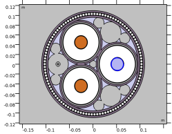
Browse to the model’s Application Libraries folder and double-click the file submarine_cable_01_introduction.mph.
|
|
3
|
|
4
|
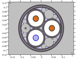
Browse to a suitable folder and type the filename submarine_cable_02_capacitive_effects.mph.
|
|
1
|
|
2
|
|
3
|
|
4
|
Browse to the model’s Application Libraries folder and double-click the file submarine_cable_c_elec_parameters.txt.
|
|
1
|
|
2
|
|
3
|
|
4
|
|
5
|
|
1
|
|
2
|
|
3
|
|
1
|
|
2
|
|
3
|
|
4
|
|
5
|
|
1
|
|
2
|
|
1
|
|
1
|
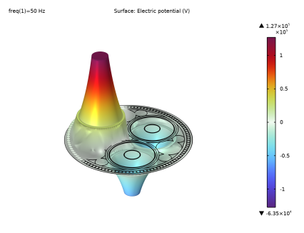
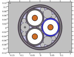
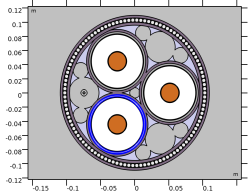
In the Model Builder window, under Component 1 (comp1) right-click Electric Currents (ec) and choose Ground.
|
|
3
|
|
1
|
|
2
|
|
3
|
|
4
|
|
1
|
|
2
|
|
3
|
|
4
|
|
5
|
|
1
|
|
2
|
|
3
|
|
4
|
|
5
|
|
1
|
|
2
|
|
3
|
|
4
|
|
5
|
|
1
|
|
2
|
Click OK.
|
|
1
|
|
2
|
|
3
|
|
1
|
|
2
|
|
1
|
|
2
|
|
3
|
|
4
|
|
5
|
|
1
|
|
2
|
|
3
|
|
4
|
|
5
|
|
1
|
|
2
|
|
3
|
|
1
|
|
2
|
|
3
|
|
1
|
|
2
|
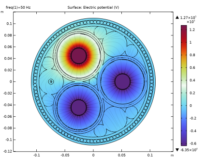
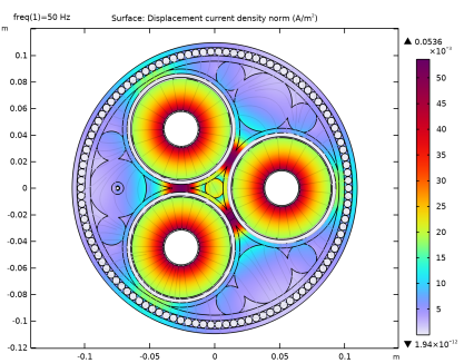
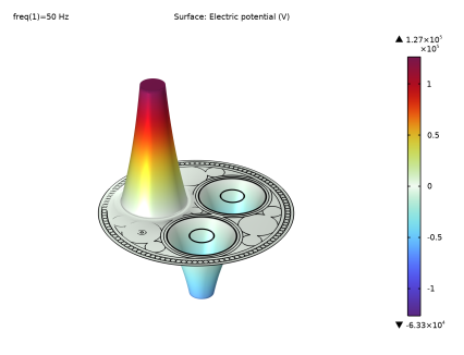
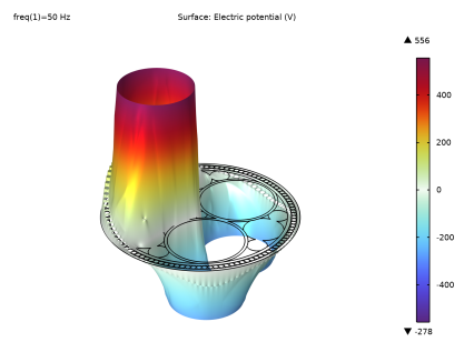
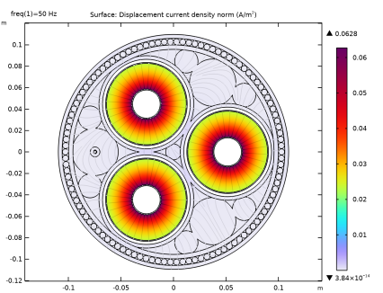
In the Settings window for 2D Plot Group, type Displacement Current Density Norm (ec) in the Label text field.
|
|
1
|
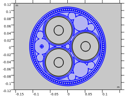
In the Model Builder window, expand the Displacement Current Density Norm (ec) node, then click Surface 1.
|
|
2
|
|
3
|
|
4
|
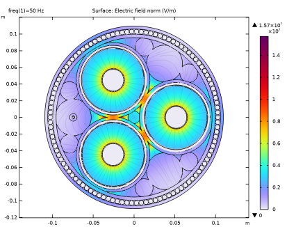
Select the Description check box. In the associated text field, type Displacement current density norm.
|
|
1
|
In the Model Builder window, expand the Results>Displacement Current Density Norm (ec)>Streamline 1 node, then click Color Expression 1.
|
|
2
|
|
3
|
|
4
|
|
5
|
|
1
|
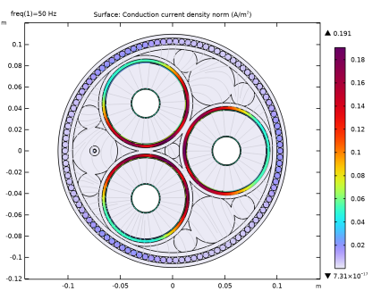
In the Model Builder window, right-click Displacement Current Density Norm (ec) and choose Duplicate.
|
|
2
|
In the Settings window for 2D Plot Group, type Conduction Current Density Norm (ec) in the Label text field.
|
|
1
|
In the Model Builder window, expand the Conduction Current Density Norm (ec) node, then click Surface 1.
|
|
2
|
|
3
|
In the Expression text field, type sqrt(abs(ec.Jix)^2+abs(ec.Jiy)^2), that is, replace “d” with “i”.
|
|
4
|
|
1
|
In the Model Builder window, expand the Results>Conduction Current Density Norm (ec)>Streamline 1 node, then click Color Expression 1.
|
|
2
|
|
3
|
|
4
|
|
5
|
|
1
|
|
2
|
|
3
|
|
1
|
|
2
|
|
3
|
|
1
|
|
2
|
|
3
|
|
4
|
|
5
|
|
7
|
|
1
|
|
2
|
|
1
|
|
2
|
|
3
|
|
1
|
|
2
|
|
4
|
|
1
|
|
2
|
|
3
|
|
1
|
|
2
|
|
4
|
|
1
|
|
2
|
|
3
|
|
1
|
|
2
|
|
4
|
|
1
|
|
2
|
|
1
|
|
2
|
|
3
|
|
4
|
|
1
|
|
2
|
|
3
|
|
1
|
|
2
|
|
3
|
Locate the Expressions section. In the table, enter the following settings:
|
|
4
|
Click
|
|
1
|
Go to the Table window.
|
|
1
|
|
2
|
|
3
|
Locate the Expressions section. In the table, enter the following settings:
|
|
4
|
Click
|
|
1
|
Go to the Table window.
|
|
1
|
|
2
|
|
3
|
|
4
|
|
1
|
|
2
|
|
3
|